
Electrical memory effects are defined as changes in amplitude and phase of distortion components caused by modulation frequency. There are several ways of measuring memory effects. One of the most common is to plot the phase and amplitude of the distortion parameters with respect to the tone spacing in a two-tone test. A memory-less device will present a flat response versus tone spacing. Usually this method is applied to the third-order intermodulation (IM3) components of the signals. Measuring the amplitude of the intermodulation components is rather straightforward, whereas measuring their phase requires a much more elaborate setup.3
This article concentrates on the measurements of the amplitude of distortion components versus tone spacing and evaluation of the electrical memory effect for a W-CDMA signal.
It is expected that if the amplitude transition of the distortion products can be made as smooth as possible, no dramatic phase changes will happen.
The study has been carried out on a 180 W high power push-pull transistor. The focus of this investigation is not only on IM3 components but also fifth- and seventh-order components, as they become a non-negligible source of distortion for wide instantaneous bandwidth signals. The video (or instantaneous) bandwidth of a signal is defined as the difference between the lowest and highest frequency components of the usable signal. In a typical UMTS application, operators transmit four carriers. This corresponds to four adjacent slots of 5 MHz, each containing a 3.84 Mcps carrier. Consequently, the video bandwidth for such a signal is 20 MHz.
Evaluation of Memory Effects on the MRF5P21180
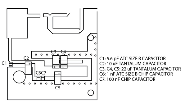
The starting point for the analysis is the LDMOS HV5 MRF5P21180 test circuit. As the study concentrates on memory effects, only the bias feed structure for the device is shown in Figure 1 .
This bias feed is repeated identically, as a mirror image, on the other side of the push-pull. It incorporates a standard quarterwave line and several decoupling capacitors - 5.6 pF for the RF, and 1 nF, 100nF, 10µF and 22 µF for the modulation bandwidth. This structure presents both very high impedance at RF frequency of 2.14 GHz and very low impedance at the modulation frequency (all frequencies up to 20 MHz).

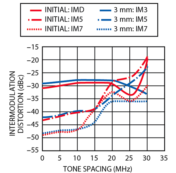
The high impedance at RF is required in order to prevent the RF from being dissipated in the DC feed section of the test circuit. The low impedance at the modulation frequency is needed to minimize the memory effect. The response of this bias network has been measured versus tone spacing for a two-tone signal of 90 W average power (180 W PEP). The measurement results are shown in Figure 2 .
As demonstrated, the decoupling circuit has a limited modulation frequency response. The IM3 and IM5 responses start to slightly degrade at very low frequencies.
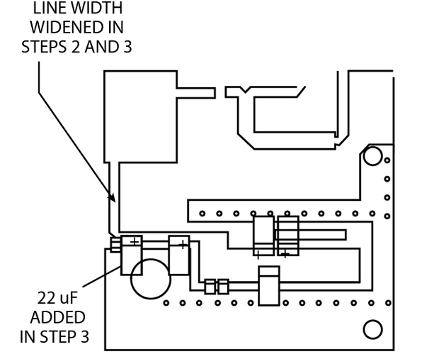
The IM5 products start to degrade sharply around 15 MHz and begin to be the main nonlinearity contributors at 20 MHz tone spacing. Also, the IM3 products show a significant variation between 20 and 30 MHz. The circuit was then modified in order to reduce memory effect. The first and main effort was concentrated on reducing the feed impedance at low frequencies. A second step consisted of widening the drain feed bar. Doubling its size from 1.5 to 3 mm, as shown in Figure 3 , yielded the blue lines on the measurement figure.
Continuing to widen the line to 5 mm and adding a 22 µF decoupling capacitor close to the RF short provided the best instantaneous bandwidth results, as illustrated in Figure 4 . As can be seen from this graph, the degradation of IM products has been pushed out beyond 20 MHz tone spacing. Also, the transitions are less abrupt. It is important to note that the lower frequency tone spacing IM3 has been degraded by approximately 2 dBc up to 15 MHz; however, no degradation in performance was noted with a W-CDMA-modulated signal input.
In addition, the same changes on the gate side do not affect the instantaneous bandwidth. This was expected because the LDMOS gate is voltage-controlled and draws no significant DC current. Most of the electrical memory effect is on the current drawing drain feeds.
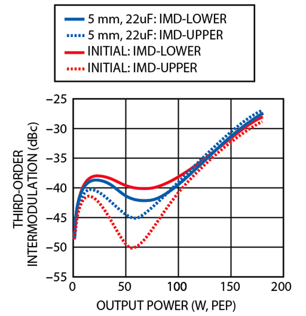
Third-order intermodulation as a function of output power at 10 MHz tone spacing is shown in Figure 5 . The improvement in instantaneous bandwidth is further exemplified by the reduction of the difference between the upper and lower IM3.

The test fixture with a wider drain feed bar shows a reduced IM3 difference of less than 3 dB. The upper and lower fifth- and seventh-order intermodulation products in the same test fixture are also illustrated in Figure 6 .
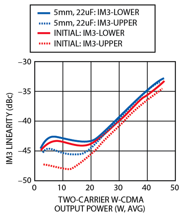
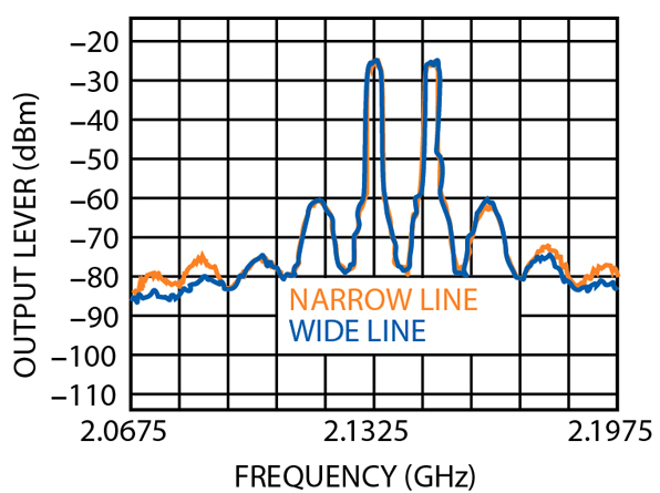
The same improvement between the lower and upper IM3 can also be observed under a two-carrier W-CDMA test signal, as shown in Figure 7 . In the design with the wider drain bias structure, the results show the IM3 imbalance is less than 2 dB. For the original bias feed design, this imbalance is 5 dB. This effect might be better visualized by plotting the spectrum analyzer response over a wide range of output power levels. A snapshot at 38 W average power is displayed in Figure 8 . From this plot, it can be seen that the intermodulation of the two carriers is more balanced with the new feed structure. Also, the IM5 and IM7 of the two-carrier W-CDMA signals are reduced, thereby putting less demand on the pre-distorter error correction circuit.
Conclusion
This study has shown that a proper biasing structure on the drain feeds of LDMOS devices can bring better instantaneous bandwidth, thereby improving memory effects.
This results in better balanced lower and upper intermodulation products, as well as reduced fifth- and seventh-order nonlinearities. These improvements put less burden on the linearizer characteristics and allow better correction at the system level.
As the mechanisms that contribute to memory effects are better understood and analyzed, means to reduce them will gradually emerge leading to less complex, less costly and more efficient linearization techniques.
References
1. J. Kim and K. Konstantinou, "Digital Pre-distortion of Wideband Signal Based on Power Amplifier Model with Memory," Electronics Letters , Vol. 37, No. 23, November 2001.
2. P. Kennington, High Linearity RF Amplifier Design , Artech House Inc., Norwood, MA 2000.
3. J. Vuolevi, T. Rahkonen and J. Manninen, "Measurement Technique for Characterizing Memory Effects in RF Power Amplifiers," IEEE Transactions on Microwave Theory and Techniques , Vol. 49, No. 8, August 2001.