

The number of mobile users is predicted to reach 1.7 billion by the year 2010. More than 45 percent of them will use high data speed services.
W-CDMA, proposed by IMT2000, has become the most practical and important system for the development of new wireless communications.
Nevertheless, second generation (2G) wireless communication systems networks are widespread and complicated.

Without compatibility, however, third generation (3G) communication systems will be an advanced technique for which acceptance and usage will be resisted.
Therefore, compatibility with 2G systems has become one of the most indispensable prerequisites to the wide implementation of 3G systems applications.

Considering the relationship between core networks and extended advanced communication systems, it is clear that the W-CDMA system is based on GSM-MAP, while the cdma2000 system is based on the ANSI-41 system.
Therefore, W-CDMA would ensure a seamless evolution from present 2G systems towards 3G systems, with the flexible wireless protocol supporting the service to users all over the world.
The idea of a multi-mode handset is currently a popular topic within the wireless communication community. Some articles concentrating on dual system handsets are currently available.1,2 Several integrated circuit device manufacturers have designed or are designing chips for the multi-mode handset.
The idea for a tri-band and dual-mode handset, covering W-CDMA/GSM/DCS systems, is suitable for the flourishing wireless communication market worldwide.

This article focuses on the design of a W-CDMA/GSM/DCS tri-band and dual-mode RF module.
A direct modulation transmitter and traditional superheterodyne receiver with integrated phase-lock loops and a controlling unit using a microprocessor unit (MPU) is developed and realized.
Design and Simulation
In order to make the single RF module applicable to several different communication systems with small size and good performance, its design should use as many common signal links for different systems as possible.
In addition, LOs, RF and IF frequencies require careful selection.
The idea of commonality is illustrated in Figure 1 . The quadrature modulator, variable gain amplifier (VGA), front-end and quadrature demodulator are used in common among the multi-modes. If the frequencies of the LOs are assigned cleverly, some IF SAW filters can also be used in common.
For the sake of finding a realizable method to make the best of both worlds under the actual conditions of the communication systems, the design of the tri-band and dual-mode RF module for a W-CDMA/GSM/DCS handset has been considered in detail.
There are several points to be taken into account, especially the size and cost of the module, since the need for such modules will be great.
First, in the transmit link, the direct RF modulation method is adopted. Consequently, it is reasonable for the two modes to have one mutual quadrature modulator with two bands around 2 GHz and 900 MHz, which can reduce the number of the devices used in the module.
Then there is no need for large and expensive IF SAW filters, which may cause a poor EVM of the transmitted signal. The system can enjoy a very low noise floor, low amplitude and phase errors in the balance between I and Q signals, and excellent carrier suppression and sideband suppression from the simplification of the circuits, compared to the complicated superheterodyne transmitters.
The two modes also use one variable gain amplifier with a suitable impedance match for both bands to adjust the level of the signal from the modulator to obtain the large dynamic range required by RF specifications. RF switches should be used to separate the signals of the two modes after the VGA and direct them into the respective power amplifiers.
Second, in the receive link, the superheterodyne receiver method is adopted to get enough signal gains and enough suppression of unwanted interferences. To obtain the dynamic range and sensitivity of the receiver, LNAs with a variable gain or step gain and mixers with high IIP3 are required.
To simplify the circuit, the two modes use one common front-end, which has two LNAs and two tri-band mixers. Then the IF signals are led into the respective IF SAW filters with suitable impedance matching circuits and then into one dual-band quadrature demodulator. Demodulators with large baseband signal gain and calibration are preferred to eliminate the baseband amplifier.

Referring to the frequency bands of these communication systems, several frequency synthesizers are needed. Integrated phase-lock loops (PLL) are used to reduce the size and cost of the module.
For the time-multiplexing of W-CDMA, GSM and DCS systems, at most three local oscillators are used at the same time. Two dual-loop PLL integrated chips are required. The details are shown in Figure 2 .
The controlling part of the module is also very important and quite complicated. Therefore, an MPU is used to realize the switching between the two modes.
The control signals include data, clock and enabling signals for the frequency synthesizers, the enabling and automatic power control (APC) signals for the transmitter, the enabling, AGC and linearity control signals for the receiver and so on.
In order to have a rough view of the performance of this system, simulations have been made using ADS software. The specifications of the channel power, ACLR, EVM and sensitivity have been simulated.
The simulation results of W-CDMA ACLR with 5 MHz and 10 MHz channel spacing are shown in Figure 3 .
To understand the sensitivity level of the module, a relationship between the bit error rate (BER) and signal-to-noise ratio (SNR) is used, which shows that in the case of QPSK modulation, if a BER of 0.001 is required, the SNR of the receiver must be above 7 dB.
If a spectrum analyzer is used to test the demodulated signal, Equation 1 can be used:


When  is obtained using the tested SNR it can be compared to the specification given to know whether the system has the proper sensitivity level.3,4
Experiment and Test Results
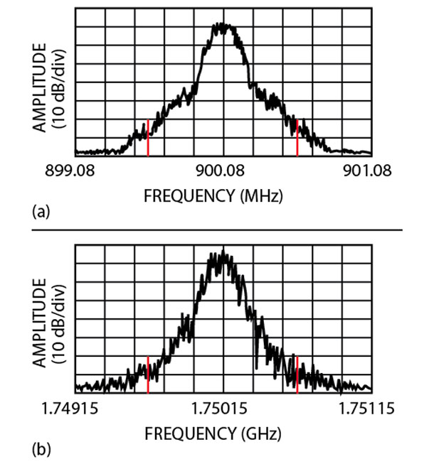
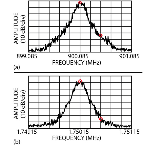
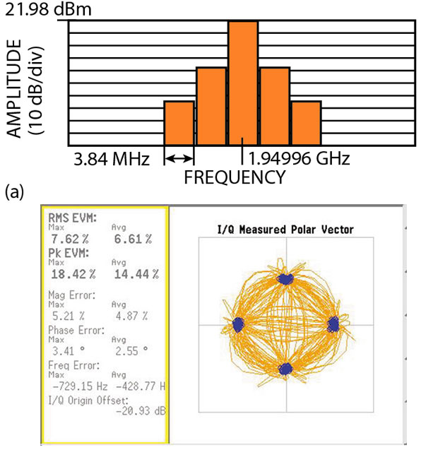
The entire RF module was integrated on a six-layer PCB. The prototype is shown in Figure 4 . It was tested with an Agilent 4433B ESG, 8594E spectrum analyzer and E4406A VSA. The transmission RF spectrums of the two modes are shown in Figure 5 . The ACP of GSM and DCS signals are shown in Figure 6 . The spectrum and the single tone test of the W-CDMA signal is shown in Figure 7 . The ACLR and EVM of the W-CDMA signals are shown in Figure 8 . The SNR of the demodulated signals of the W-CDMA mode under different received signal levels is shown in Figure 9 .
The EVM of the received W-CDMA signals with blockings and interferences is shown in Figure 10 .

According to the experiment, when the injected signal is -102 dBm, and the measured SNR is 1.27 dB, the can be calculated from Equation 1:
NF = (-102 + 174 -65.84 -1.27 + 3)
dB = 7.89 dB and
= 6.02 dB -25 dB + (-174 dBm/ Hz) +7.89 dB +7 dB +10 log (3.84 MHz) = -112.25 dBm/3.84 MHz
The sensitivity has a margin of 5.55 dB to -106.7 dBm/3.84 MHz as required by the 3GPP standard.
Conclusion
The design of an RF module for a multi-mode handset, to be used as a bridge between 2G and 3G systems, has been characterized, and a prototype of the W-CDMA/GSM/DCS tri-band and dual-mode handset has been developed and built. The prototype has been tested and has met the performance required by the 3GPP standard.3,4
References
1. M. Bailey and P. Hagstrom, "An Integrated Front-end for Multi-mode Handsets," 2000 IEEE IMS Digest , pp. 1269-1272.
2. X. Zhu, W. Hong, J. Liu, L. Tian and J. Zhou, "The Module Design for W-CDMA/GSM Dual-band and Dual-mode Handsets," 2001 IEEE IMS Digest , pp. 2215-2218.
3. 3GPP TS 25.101 V3.5.0 UE Radio Transmission and Reception (FDD).
4. 3GPP TS 05.05 V8.10.0 Digital Cellular Telecommunications System (Phase 2+).