
The W-CDMA standard expresses transmit quality in terms of EVM and ACLR, and receive quality in bit error ratio (BER). These quality measurements are simple scalar numbers representing a very complicated system.
Modern communications channels (still) consist of a number of concatenated functions such as baseband (BB) processor, DAC, modulator and amplifier. Each function contributes to the global figure of merit. A method needs to be found to capture the performance of each block in a behavioral model that, when concatenated, gives useful and accurate information on the overall system performance. The behavioral model of each block may be generated either from precise (circuit-based) simulation or by measurement.

An advantage of a behavioral model is the more compact representation it provides for a circuit, allowing the circuit to be simulated much more quickly, using less memory. This makes it more desirable for doing higher level circuit or system design. Since a component can be treated as a block and an equivalent circuit structure does not need to be known, it is potentially easier to generate a behavioral model than a circuit model. Another advantage is that a component vendor can supply a behavior model to designers without giving away any information about the details of the device.
Behavioral models based on circuit simulation are limited to the accuracy of the underlying circuit model. However, a behavioral model may be based on measurements of the component, and has the advantage of capturing the actual nonlinear performance of the device. In order to get models that are of more general purpose, the devices need to be measured with a more complex stimulus to more fully characterize their nonlinear behavior. Electronic signal generators (ESG) and vector signal analyzers (VSA) can be used to generate these complex test signals, and capture the complex modulated response, from which the data to populate a behavioral model may be obtained.
This article extends the concept of behavioral modeling by creating a model structure for baseband I/Q-to-RF modulators, along with using real-world measurements as a method for filling in the data for such a model.
Gray Box Modeling
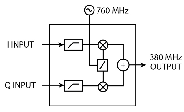
The term "gray box" is used to describe a model whose structure is known, but the details are not. In this case, it is assumed that the model maps I/Q inputs to modulated RF outputs, and the model details the transfer function. In this model, the linear distortion effects (such as filtering) are separated from the nonlinear distortion effects. Thus, the behavioral model for the nonlinear effects is required to be memory-less. A memory-less assumption also implies a flat frequency response, and no PM-to-AM conversion. The frequency response effects of the input I/Q filtering will be represented by a linear frequency dependent element before the nonlinear element.
Figure 1 shows the behavioral model for the modulator. The I/Q input filters (which are caused by DC blocks and baluns in the test fixture) were evaluated using an ESG that has an arbitrary waveform generator (AWG) for the baseband I/Q signals. A stepped sine wave was created for each of the I/Q inputs, and the output RF power measured on a VSA. Figure 2 shows the frequency response of the I input (Q is similar) as well as the modeled response for a filter function used in the behavioral model.
What is desired for the nonlinear transfer function is a function that describes the RF output amplitude and phase as a function of the I and Q voltages. A simple way of doing this might be to drive a DC voltage into I, and measure the RF output (magnitude and phase) for various input levels, then repeat the same measurement for Q. However, I and Q may have some interaction, so the next level of stimulus to consider is setting I to a particular level, then vary Q over a range of values, while measuring the RF output; this would be repeated for a variety of I values. Unfortunately, from the I and Q input response, it is clear that the response goes to zero at DC (the I and Q are DC blocked).
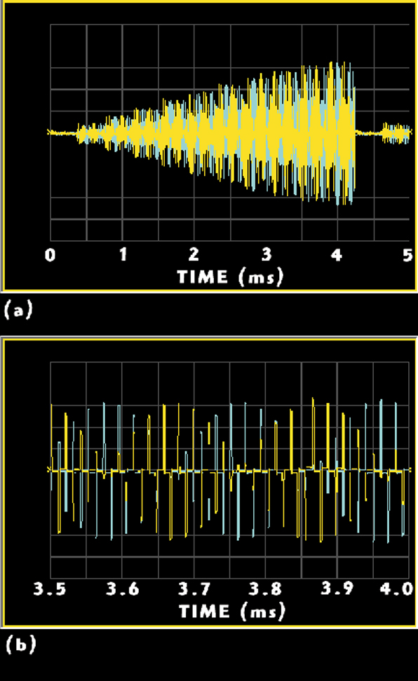
A specialized drive of I and Q to measure the transfer function is required. After much experimentation, a pulsed DC signal was determined to be the best-suited drive. The magnitude of I and Q, (M = √(I2 +Q2)), is held constant and the phase is changed in 170° increments until 36 data points (every 10°) is obtained. By changing the phase 170°, any charging of the blocking capacitor is nearly removed by the next pulse. Figure 3 shows the input signal, as measured on a VSA using the I/Q baseband inputs. The pulse was filtered to maintain a frequency content consistent with a W-CDMA signal, using a low pass filter of 2 MHz bandwidth. The spacing between pulses was set to allow any residual charge to leak off before the next pulse arrived. The last part of the stimulus is shown expanded, with I in yellow and Q in blue.
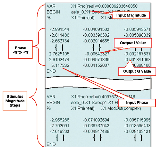
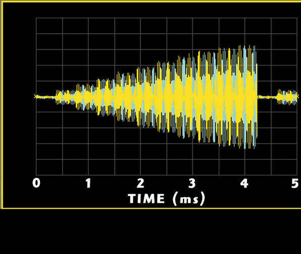
Figure 4 shows the output of the modulator, measured on a VSA using the RF input. The output modulated I/Q is compared to the input, and a transfer function is determined. This transfer function is used to populate a behavioral model that relates the input I/Q (magnitude and phase) to the output RF envelope. Figure 5 shows the behavioral model data used as an input to the simulation. A behavioral model simulation was created and the original pulsed input was used as a simulation stimulus. The response produced an output nearly identical to the measured output. Next, the model was stimulated with a W-CDMA signal, and the EVM response was obtained. As shown in Figure 6 , there was remarkable agreement with an actual measurement of EVM on the modulator. A similar process was used to characterize an RF amplifier, with the characterization consisting of measuring the amplitude and phase compression from which a behavioral model of the amplifier was created.

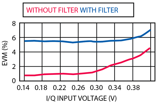
The DC blocking of the I/Q is a result of the test fixturing. The goal was to determine the response of the modulator without the DC block, but such a measurement was not possible. However, the filtering function in the simulator could be de-embedded, and a complex modulation signal applied to the resulting model. Figure 7 shows the result of this experiment. The DC block has a strong effect on EVM, and it can be clearly seen that the degradation of EVM of the modulator, although small, occurs at a much lower input drive that the preceding figure would indicate.
Finally, the modulator and amplifier were cascaded, both physically and in the simulation, and the measured and simulated EVM of the cascaded pair was compared. Figure 8 shows this result. Similar comparisons were done for other modulated characteristics such as adjacent channel power ratio (ACPR) and alternate channel power ratio, with good results.
Conclusion
For the first time, a method for creating measurement-based behavioral models has been presented as related to I/Q modulators. The model was validated using measurements of W-CDMA signals. Furthermore, the cascading of behavioral models was tested against a modulator and amplifier combination, and found to correctly predict the response to a complex modulated signal.
References

1. Connected Simulation and Test Solutions Using the Advanced Design System, Agilent Technologies, Application Note Number 1394, Lit Number 5988-6044EN.
2. "3GPP W-CDMA Systems: Design and Test," IEEE Microwave Magazine , June 2002; http://ieeexplore.ieee.org/iel5/6668/ 21676/01004052.pdf.
3. "The State of Wireless Networking Simulation and Verification," Applied Microwave and Wireless ; www.amwireless.com/ archives/2001/v13n12/v13n12pg106.pdf.
4. The Design and Verification of IEEE 802.11a 5 GHz Wireless LAN Systems; http://www.chipcenter.com/networking/images/technote/ technote019.pdf.
5. Blending Test Equipment into the Design Mix to Generate Custom, Real-world Waveforms (cdma2000); http://www.chipcenter.com/networking/technote/Agilent _Wave_Synth/.
6. Terminal Conformance Specification; Radio Transmission and Reception (FDD) (Release 1999), 3GPP Technical Specification 34.121, v3.0.0 (2000-3); http://www.3gpp.org.
7. Agilent Solutions for Designing and Manufacturing Base Transceiver Stations and Their Components; http://www.agilent.com/find/ basestationtest.
8. Agilent Solutions for Designing and Manufacturing Wireless Appliances; http://www.agilent.com/find/wirelessdesign.
9. Agilent 3G Application Notes; http://www.agilent.com/find/3G.
10. Agilent ADS Training Class: Designing W-CDMA/3GPP Communication Systems Using ADS; http://contact.tm.agilent.com/tmo/ eesof/education/.
 Joel Dunsmore received his BSEE and MSEE degrees from Oregon State University in 1982 and 1983, respectively. He is currently a senior design engineer working as a solution architect for the Component Test Market Solutions unit of Agilent Technologies (formerly Hewlett-Packard) at the Sonoma County site. He was a principle contributor to the HP 8753 and HP 8720 family of network analyzers, responsible for RF and microwave circuit designs in these products. He holds six patents related to this work, has published numerous articles on measurement technology, and consults on measurement applications. He has taught electrical circuit fundamentals and presented several short courses and seminars through ARFTG, MTT and HP.
 Greg Jue is a communications system application specialist at Agilent EEsof. He is the product manager for the ADS 3GPP W-CDMA design library, and also specializes in ADS links to Agilent test equipment. He created the ADS 3GPP W-CDMA course and ADS Communications System Design course, and has taught numerous RF circuit design, communications system design and 3GPP W-CDMA design courses using ADS. He has been with Agilent EEsof for six years, and was at the Jet Propulsion Laboratory/Caltech University working on system design for the Deep Space Network prior to joining Agilent Technologies.
 John Kikuchi graduated from the University of California at Berkeley School of Engineering in 1979. He then joined the US Air Force as a research engineer. He is currently a solution planner for the Wireless Business Unit of Agilent Technologies, where he has worked since 1983. His experience at Agilent also includes work in R&D, QA, and, most recently, sales and marketing for Agilent EEsof EDA.