
Modern commercial and military communication systems require high efficiency, long term operating conditions. For this purpose, the power amplifiers, as final and highly current-consuming transmitter elements, are developed using the high efficiency class B, F or E modes of operation, depending on the technical requirements.
In class B operation, which is a special case of class C with a conduction angle of half a period, the collector voltage waveform is pure sinusoidal and harmonics are present in the collector current only. In class F power amplifiers, the fundamental and harmonic load impedances are optimized by using short-circuit termination and open-circuit peaking, in order to control the collector voltage and current waveforms to obtain maximum efficiency. In class E amplifiers, an efficiency improvement is achieved by realizing the on/off switching operation with special current and voltage waveforms so that high voltage and high current do not exist at the same time. And if both collector voltage and current waveforms in an idealized class E mode contain all of the harmonics, then in class F only a certain amount of harmonic content is needed for either collector voltage or current waveforms. For example, only odd harmonic components are necessary to realize the ideal collector voltage form, and even harmonics components to form the ideal current one. As a result, the impedance conditions are different when, for class F operation, there is need to create zero or infinite impedance at any harmonic component, whereas for class E operation, all reactances at the harmonics should be negative.
At first glance, it looks like these high efficiency operation modes do not have anything in common with each other since it is necessary to provide different impedance conditions as well as to apply different circuit design approaches. However, to approximate class F or E modes, it is enough to realize the required impedance conditions only for several harmonics1 and, more importantly, to apply the same circuit design technique - one or several harmonically tuned parallel circuits or only one parallel circuit mistuned at the fundamental frequency. All that is needed to design a high efficiency RF power amplifier is the proper choice of the parameters of the load network parallel circuit.
Class B

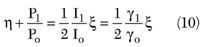
The equivalent circuit of a class B power amplifier with a parallel resonant circuit is shown in Figure 1 , where Cb is the blocking capacitance. The voltage and current waveforms for the active device operating in active and cut-off modes are also shown. The presence of an ideal parallel circuit, tuned at the fundamental frequency, leads to a sinusoidal collector voltage giving a sinusoidal current flowing into the load resistor R, while all harmonic current components are flowing through this parallel circuit having an infinite impedance at the fundamental and zero impedance at all harmonics. If the output device impedance at the required output power level is different from a 50 Ω load, then it is necessary to incorporate a matching circuit with the appropriate impedance ratio between the parallel circuit and the load.
Analytically, class B operation can be written as

where
Iq = quiescent current
I = fundamental current amplitude
Θ = conduction angle part of the RF current cycle, for which the device conduction occurs and determines the point in time when the collector current ic takes a zero value
At this moment
ic = 0 = q + IcosΘ (2)
and the conduction angle Θ can be calculated from

Consequently, in a common case
ic = I(cosωt - cosΘ) (4)
When ωt = 0, the collector current has a maximum amplitude of
ic = Imax = I(1 - cosΘ) (5)
From Equation 3 one can obtain the following basic definitions: when Θ> 90°, then cosΘ < 0, Iq > 0 corresponding to class AB operation; when Θ = 90°, then cosΘ = 0, Iq = 0 corresponding to class B operation; when Θ < 90°, then cosΘ > 0, Iq < 0 corresponding to class C operation.
As a result, the periodic half-cosinusoidal output current ic could be represented as a Fourier series expansion
ic = I0 + I1cosωt + I2cos2ωt + I3cos3ωt + ... (6)
where the DC, fundamental and harmonic components can be obtained from


where

Consequently, in contrast to the class A operation mode where Θ = 180° and the DC current is equal to the quiescent current during the whole period, for the other above-mentioned operating modes with Θ < 180°, the DC current component is a function of the conduction angle Θ.
The collector efficiency of a class B power amplifier, with an output power P1, can be obtained from
where
ζ = V/Vcc is the collector voltage peak factor
If ζ = 1 and Θ = 90°, then from Equation 8 it follows that the maximum collector efficiency in class B operation is

CLASS F
As can be seen from class B operation, only one parallel circuit tuned at the fundamental frequency results in insufficient high efficiency operating conditions. Additionally, Equation 11 represents the maximum ideal value, which is unrealizable in practice. Therefore, it is advisable to consider more efficient operation modes, which can ideally provide 100 percent collector efficiency.
First, consider the idealized load network harmonic conditions for class F operation2

Zn = 0Ω for even n
Zn = ∞Ω for odd n (12)
where
R = load
n = harmonic component

The ideal voltage and current shapes corresponding to the impedance conditions given by Equation 12 are shown in Figure 2. Here, a sum of odd harmonics gives a square voltage waveform and a sum of even harmonics approximates a half-sinusoidal current shape. Based on the analysis of the square voltage and half-sinusoidal current waveforms, it is necessary to provide a peaking of several current and voltage harmonic components in order to achieve a high value of power amplifier efficiency. The better flattening of the voltage waveform provided by high order harmonic components, the less power dissipation is due to the flow of output current when the output voltage is extremely small. To understand the common design principles and to calculate numerically the power amplifier efficiency depending on the appropriate number of the frequency harmonic components of voltage and current waveforms, it is advisable to use a design technique applied to class F approximation with maximally flat waveforms.3,4
For example, an ideal class F amplifier with only the second harmonic voltage short-circuited and one third-harmonic current peaked realizes a maximum drain efficiency of 75 percent. In this case, for maximum voltage waveform flatness, the fundamental and third-harmonic voltages should be out-of-phase as shown, and the optimum ratios between voltage and DC current and appropriate harmonic components must be
However, as follows from Equation 9, the current coefficient Θ3Θ becomes negative only for conductance angles of Θ > 90°, which means class AB operation for a power amplifier with more than 50 percent duty cycle. There are also several other possibilities, like using a slightly overdriven operation with a non-sinusoidal collector current waveform, including an out-of-phase third-harmonic, or using a non-sinusoidal driving signal containing the third-harmonic at the required amplitude. Nevertheless, in practice, due to the inherent active device nonlinearity, it is enough to choose a class AB mode with a small quiescent current, which is a compromise between power amplifier high efficiency and high gain operation.
The load network design approach for a high efficiency power amplifier can be based completely on using parallel resonant circuits tuned at the required harmonic frequency component. For example, to realize an idealized collector efficiency of 88.4 percent, it is necessary to incorporate an additional parallel circuit L3C3 realizing the infinite impedance at the third-harmonic current component, as shown in Figure 3. In this case, a zero impedance at the second, fourth and higher harmonic components is assumed. The harmonic currents are flowing through the resonant circuit L1C1 tuned at the fundamental. Further efficiency improvement up to 92 percent can be made with the additional resonant circuit L5C5 connected in series to the collector terminal and tuned at the fifth current harmonic component. At microwave frequencies, all these lumped parallel circuits connected in series should be replaced by a quarter-wave transmission line short-circuited at the output. Such a circuit can ideally provide 100 percent collector efficiency, due to zero impedance at even harmonics and infinite impedance at odd harmonics. By having its characteristic impedance differ from the load, this transmission line can also realize the impedance transformation.
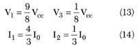
In reality, both extrinsic and intrinsic transistor parasitic elements have a substantial effect on the efficiency, especially at high frequencies. First, it is necessary to take into account the main influence of the device output capacitance Cout, the collector capacitance Cc for a bipolar device, or drain-source capacitance Cds for an FET device. For a lumped-circuit power amplifier, in order to approximate the ideal class F with harmonic impedance conditions of Z1 = Z3 = ∞Ω and Z2 = 0 Ω at the device output terminal by compensating the influence of Cout, it is also advisable to use an additional parallel circuit L2C2 connected in parallel, as shown in Figure 4, where the series resonant circuit L0C0 is tuned at the fundamental. As a result, the optimum ratios between the circuit elements can be calculated from4,5

In order to increase maximum efficiency up to 88.4 percent, it is necessary to provide a short-circuit termination for all even harmonic voltage and an open-circuit impedance for the third-harmonic current. Such a class F operation mode is easy to realize by using transmission lines in the output circuit when one of them is connected in parallel to the active device between the output device terminal and voltage supply. Such a circuit schematic is the dual to the one shown in the previous figure, when the transmission line is connected in series, but is more acceptable for practical implementation since no additional losses are due to the RF current at the fundamental frequency. Thus, for such a microstrip power amplifier, it is quite enough to provide the following electrical lengths of the transmission lines at the fundamental frequency4,5

where
Z0 = characteristic impedance of each microstrip line
Class E
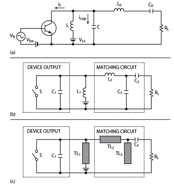
Switched-mode class E tuned power amplifiers are widely used in different frequency ranges and output power levels beginning from several kilowatts at low RF frequencies to approximately one watt at microwave frequencies. In such class E power amplifiers, the load network usually consists of a shunt capacitance and a series inductance, which allow operating the transistor as an on-off switch under optimum values of load network elements.6 The ideal shapes of the collector current and voltage waveforms demonstrate a condition when the high current and high voltage do not overlap simultaneously, that minimize the power dissipation and maximize the power amplifier efficiency up to 100 percent. However, such a load network configuration is not unique. For example, the switched-mode class E tuned power amplifiers with a parallel circuit, shown in Figure 5, can be an alternative to the class E tuned power amplifiers with a shunt capacitance, also realizing the high efficiency operation mode.4,7 The load network with a parallel circuit consists of a parallel capacitance and a parallel inductance with an additional series filtering circuit to provide a high level of harmonic suppression.
The basic circuit of a switched-mode tuned parallel-circuit class E power amplifier is shown in the diagram. The load network consists of a parallel inductance L, a parallel capacitance C, a series L0C0 resonant circuit tuned at the fundamental frequency ω0 = 1/√L0C0 and a load R. In a common case, a parallel capacitance C can represent the intrinsic device output capacitance and the external circuit capacitance added by the load network. The active device is considered to be an ideal switch that is driven in such a way as to provide the device switching between its on- and off-state operating conditions. The loaded quality factor QL of the series resonant L0 C0 circuit should be high enough for the output current to be sinusoidal.

The normalized collector (a) current and (b) voltage waveforms for an idealized optimum parallel-circuit class E operating mode are shown in Figure 6. From the collector voltage and current waveforms, it follows that, when the transistor is turned on, there is no voltage across the switch and the current ic consisting of the load sinusoidal current and an inductive current flows through the device. However, when the transistor is turned off, this current now flows through the parallel capacitance C. As a result, there is no nonzero voltage and current simultaneously, which means a lack of power losses and gives an idealized collector efficiency of 100 percent.
The optimum load network parameters can be obtained from4,7

whereas the optimum load resistance for the specified values of supply voltage Vcc and output power Pout, taking into account that R = VR2/2Pout, can be calculated from

The phase angle between the fundamental frequency voltage and current seen by the switch terminal is equal to
Φ= 34.244° (20)
which means that the load network is slightly mistuned with respect to the fundamental frequency and the values of the load network parameters should be chosen to create an inductive reactance at the fundamental frequency and capacitive reactances at the harmonic components.
For high power or low voltage power amplifiers, it is very important to know how small the value of the required load resistance is, since the higher its value, the easier to provide impedance matching to a conventional 50 Ω load. Thus, for the same output power with the same supply voltage, the ratio between load resistances R(B) in class B, R(F) in class F and R(E) in parallel-circuit class E can be written as4

which clearly shows that, for parallel-circuit class E power amplifiers, the design output matching procedure can be significantly simplified. If the calculated value of the resistance R for the optimum parallel-circuit class E power amplifier is too small or differs from the required load resistance RL significantly, it is necessary to use an additional matching circuit to provide maximum output power to the load. In this case, the first series element of such matching circuits should be an inductance to provide high impedance conditions for harmonics.
For a microwave power amplifier, usually all the inductances in the output matching circuit should be realized with transmission lines, in order to reduce the power losses. Therefore, for a parallel-circuit class E power amplifier, the parallel inductance L should be replaced by the short-length transmission line TL1 with the optimum parameters obtained from

where
Z0 = characteristic impedance of the transmission line TL1
Θ = electrical length of the tramission line TL18
Thus, a parallel circuit, being a very simple electrical structure, in reality represents a powerful means for increasing power amplifier efficiency operation. Therefore, in class B, the load network contains a parallel circuit tuned to the fundamental frequency providing also sufficient harmonic suppression. In class F, to approximate a 100 percent collector efficiency, one or several parallel circuits tuned at the harmonic components or a quarter-wave transmission line are used as the parallel circuit single-frequency equivalent. In class E, it is enough to use a slightly mistuned parallel circuit having an inductive reactance at the fundamental frequency and capacitive reactances at the harmonic components.
References
1. F.H. Raab, "Class E, Class C and Class F Power Amplifiers Based Upon a Finite Number of Harmonics," IEEE Transactions on Microwave Theory and Techniques , Vol. MTT-49, August 2001, pp. 1462-1468.
2. H.L. Krauss, C.W. Bostian and F.H. Raab, Solid State Radio Engineering , John Wiley & Sons Inc., New York, NY 1980.
3. F.H. Raab, "Class F Power Amplifiers with Maximally Flat Waveforms," IEEE Transactions on Microwave Theory and Techniques , Vol. MTT-45, November 1997, pp. 2007-2012.
4. A.V. Grebennikov, RF and Microwave Power Amplifiers and Oscillators: Theory and Design , Noble Publishing, 2002.
5. A.V. Grebennikov, "Effective Circuit Design Techniques to Increase MOSFET Power Amplifier Efficiency," Microwave Journal , Vol. 43, No. 7, July 2000, pp. 64-72.
6. F.H. Raab, "Idealized Operation of the Class E Tuned Power Amplifier," IEEE Transactions on Circuits and Systems , Vol. CAS-24, December 1977, pp. 725-735.
7. A.V. Grebennikov and H. Jaeger, "Class E with Parallel Circuit - A New Challenge for High Efficiency RF and Microwave Power Amplifiers," IEEE MTT-S International Microwave Symposium Digest , 2000.
8. A.V. Grebennikov and H. Jaeger, "Transmission-line Tuned Switching Power Amplifier," US patent (pending).
Andrei Grebennikov received his Dipl. Ing. degree in radioelectronics from the Moscow Institute of Physics and Technology, and his PhD degree in radio engineering from the Moscow Technical University of Communications and Informatics in 1980 and 1991, respectively. He joined the scientific and research department of the Moscow Technical University of Communications and Informatics as a research assistant in 1983. His scientific and research interests include the design and development of power RF and microwave radio transmitters for base station and handset applications, hybrid integrated circuits and MMICs of narrow- and wide-band, low and high power, high efficiency and linear microwave and RF amplifiers, and single-frequency and voltage-controlled oscillators using any type of bipolar and field-effect transistor. From 1998 to 2001, Grebennikov was a member of the technical staff at the Institute of Microelectronics, Singapore, responsible for the design and development of the LDMOS FET high power amplifier module. Since January 2001, he has been with M/A-COM Eurotec (Cork, Ireland), where he is involved in the design and development of 3G handset InGaP HBT power amplifiers and low noise VCOs.