
The quadrature demodulator is used in either heterodyne or homodyne receivers. In commercial communication receivers, the local oscillator frequency ranges from a few kilohertz to a few gigahertz. It is usual to test the individual part with a single tone to avoid the complexity of the baseband waveform.
The local oscillator could be non-coherent when the measurement is performed. This approach simplifies the tests to normal RF and IF measurements. However, the measured results should be applicable to signals occurring in normal receiver operation - the modulated passband signal and the demodulated baseband signal. In this signal processing issue, using the measured results without considering their accurate definitions would lead to errors. The correct approach is to go from baseband and passband signal processing concepts to simple RF and IF measurement approaches, which will correlate correctly the performance of the demodulator for real world signals.

Figure 1 shows the block diagram of a typical quadrature demodulator. It consists of a variable gain amplifier (VGA), mixers and baseband filters. To provide a receiver design with the demodulator performance, or to set the required demodulator specifications based on the required receiver performance, the specifications need to be made and a measurement method should be proposed. The dash line refers to the IC boundary. A number of external components are used for the test.
Receiver Design
In receiver design, the final bit error rate (BER) requirement determines the symbol carrier to interference ratio (C/I) at the demodulator output. For simplicity, it is assumed that I is uncorrelated or Gaussian and white. An example of this can be seen in the third generation WCDMA cellular system. For a BER = 10-3 , the required Eb /No is 6.8 dB for a QPSK signal.1 There is 21 dB (spreading factor 128) dispreading processing gain. The convolutional coding gain is assumed to be 4.5 dB for simplicity. The ratio of data channel power to the total received power is -10.3 dB. Therefore, the required bit C/I is 6.8 - 21 - 4.5 + 10.3 = -8.4 dB. Please note that this is the C/I for the bit. The sensitivity required is -106.7 dBm at the symbol power.1 The QPSK symbol contains two bits and when this sensitivity input level is used, the demodulator output symbol C/I that is required to achieve the BER is also -8.4 dB. The receiver chain from the antenna port to the demodulator I and Q ports is calculated for its signal level, noise level and distortion (intermodulation products) level. There are two ways to define the individual demodulator specifications, either before or after the recombination.
The receiver requirement is calculated for modulated passband and baseband signals, but the measurement is performed with a single tone. The intent of the following discussion is to identify the correlation between modulated and single-tone signals.
Measurement Set-up
This section discusses the single-tone measurement. In subsequent sections the single-tone measurement results on the actual receiver will be compared with the modulated signal ones.
The IC demodulator circuits usually begin with a differential pair of transistors as input and usually end with a differential pair of transistors as outputs for both I and Q channels, in the form of closed emitters or collectors. When the IC is used in a receiver, the input needs to be conjugate-matched, due to the noise figure cascade properties.
where


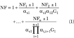
Equation 1 is the well-known noise figure cascade formula, which shows that, at the relatively early stages, the mismatch coefficient a will degrade the cascaded noise figure. A simple derivation of this equation is provided in Appendix A . The IC input RF impedance is usually a few kilohms for the differential pair. To reduce the Q of the matching circuit and to have better linearity, a parallel resistor of a few hundred ohms is added. In the receiver chain, the matching occurs between the output of the previous stage (usually filter or mixer) and the IC input impedance with a parallel resistor. For measurement, it is matched to a 50 Ω single-ended terminal. The conjugate matching implies that the power at the IC input is equal to the power at the 50 Ω test input port, whereas the voltage has been transformed between these two reference planes.
On the other hand, when the IC is used in the receiver, its output needs to be severely mismatched to save current for the larger signal and to reduce the absolute noise level in order to increase the signal-to-noise ratio. However, according to Equation 1, with the high gain product of the previous stages, the noise figure contribution of that stage is relatively small even with very small mismatch coefficients. This is why the receiver cascade noise figure and sensitivity calculation is usually only done for the parts before the mismatch begins. The excess noise of mixed-signal circuits and the digital signal processing circuits following the demodulator is usually low enough to be neglected in the process of cacading noise figures. For a certain input Si /Ni at the receiver antenna port, the input noise from the transmitter is usually required to be much lower (at least 10 dB) than the thermal noise level (-174 dBm/Hz) when the input signal level is approaching the sensitivity limit. For a certain NF of the receiver, the output S0 /N0 at the demodulator IQ ports is equal to (Si /Ni ) • (1/NF), where at worst case the Si is at sensitivity level and the Ni is at -174 dBm/Hz • BW (bandwidth). The output S0 /N0 should meet the required symbol C/I.
The IC output RF impedance is typically a few hundred ohms, and the load has a high impedance of a few tens of kilohms. The voltage gain (Gv ) of the IC demodulator is specified by the IC manufacturer for certain load conditions. However, a more useful specification for the receiver system analysis is the demodulator power gain for a matched load. There are two reasons for this. First, in the receiver system analysis, it is easy to assume a matched case for each stage when performing power gain, noise and intermodulation distortion (IMD) products cascades. To obtain a mismatched load, use the matched power gain of the demodulator and multiply it by a mismatch coefficient.
Second, it is not necessary to redo the measurement when different loads are used. If the output RF impedance of the demodulator is known, simply apply a different mismatch coefficient to calculate the voltage and power delivered to a different load.
For measurement purposes, the input and output impedances of the demodulator are shown together with the impedance transformation at the demodulator's input and output. The external op-amp is used to simulate the load and transform the high impedance to 50 Ω so the measurement can be made with a spectrum analyzer. The five impedance designators at five reference planes are also used for the rms voltage levels, except for V3, where a mismatch occurs, referring to the rms voltage when it is matched. In the following, unless otherwise specified, the impedances will always be differential and the voltages will always be the rms values.
The op-amp is designed to have unity gain because it is set to have R3 R1 = R4 /R2 = 2. The op-amp gain is 2. The post op-amp R5 is 50 >Ω to divide the voltage by 2 at the test load Z5 . Therefore, V5 = V4 . The op-amp performs an impedance transformation and simplifies the test for the spectrum analyzer.
The single-tone measurement is done the simple and usual way. The set-up can also be used to test the baseband signal waveform when the RF/IF signal is modulated. In some cases, the op-amp's balun function, frequency response and noise may need to be calibrated.
Both the input and output impedances of the IC demodulator are 500 Ω. Remember that when the output impedance is known, the load setting could be slightly different from the setting in the actual receiver. Set Z4 = R1 + R3 = R2 + R4 = 60 kΩ.
For simplicity, the following derivations assume that all impedances are resistive. Suppose the measured power gain Gp = P5 /P1 = 95 dB, which is referred to as raw gain. The IC voltage and matched power gain are easily obtained. The voltage gain of the IC demodulator is
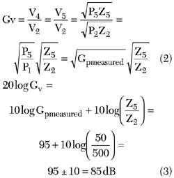
The power gain from the input of the IC to the dummy load, which is also the input of the op-amp, is


This mismatch coefficient is

The matched power gain of the IC demodulator is


This number, after the adjustment for the modulated signal, which is explained later, will be used in the receiver chain analysis for the signal, noise and IMD power.
Modulated Signal Gain

The modulated signal gain is of interest in receiver design. This section features the mapping between the modulated signal gain and the single-tone measurement. Figures 2 and 3 show the signal representations in the time and frequency domains for the modulated signal and the single-tone signal.
The quadrature demodulator can be used for many different modulation signals. The mapping between the modulation signal and the single-tone measurement is modulation-type dependent. The following discussion will focus on and use the QPSK modulation as an example. For this discussion, the analytic form is specifically for QPSK.

To simplify the analysis, it is assumed that the local oscillator is coherent. The result should not lose generality because, in the non-coherent case, although the instantaneous phase has been shifted, the overall integral for the average power is the same as in the coherent case. The signal voltage mapping or the power between modulated signal and single-tone signal is in a continuous time period, which is the average signal voltage or power.
As can be seen, the single-tone signal is at a certain offset Ω from carrier frequency ω. Normalizing the demodulator gain to unity, the single-tone demodulated signal at the I branch after low pass filtering is:

The voltage gain is 1/2 and the power gain is 1/4. The demodulated modulated signal at the I branch after low-pass filtering is

where

If the modulation is QPSK with

The voltage gain is then 1/√8 and the power gain is 1/8.
Compared to the measured single-tone power gain for the I or Q branch, the actual modulated signal power gain is 3 dB less. The recombination of I and Q QPSK signals will provide 3 dB more power as illustrated in the signal representation diagram. Therefore, the Gp measured by the single tone is equal to the modulated signal power gain after recombination. In many cases, a certain voltage range is required for V4 , which could be the input buffer of an analog-to-digital converter (ADC), making Gp - 3 dB the power gain to be used for the calculation.
Quadrature Modulated Signal
In the spectrum domain, it is obvious that the modulated signal spectrum is symmetric and the single-tone spectrum is asymmetric. Imagine that the modulated signal spectrum consists of multiple tones (the Fourier expansion), or downgrade the modulating baseband signal to a single tone. It is easy to add another tone, at ω- Ω, to the existing single tone, at ω + Ω, as shown by the dashed line in the spectrum representation.
The double tone demodulated signal is then
(cos(ω + Ω)t + cos(ω - Ω))cosωt = cos Ωt (12)
The voltage gain is 1/2, again the same as the single-tone case. Try shifting the tone phase by 90°, it becomes

which is the same as the modulated signal. So far, the mapping between the single tone and modulated signal is clarified for the quadrature nature of the signals.
Noise
The receiver design example must contain the noise figure of the demodulator for the system C/I after IQ recombination. It is easy to measure the output noise power density N0measured at either the I or Q output of the set-up and to calculate the noise figure using

where
 i = KT = -174 dBm/Hz
NFmeasured = N0measured + 174 - Gp (dB) (14-2)

This section discusses how to map NFmeasured to the actual noise figure of the demodulator.
Figure 4 shows two different cases for the demodulator and its noise. Case 1 has a VGA in the front, whereas case 2 does not have a noise source before the signal splits. For both cases, the output noise power after IQ recombination is
N0 = Ni GM p + (NF - 1)KTBGM p (15)
where
Ni = input noise power
GM p = modulated signal gain
The first part of Equation 15 is not related to the noise figure of the demodulator. The noise figure is defined as

where Ni must be KTB. It is the measure of the additional noise that is generated by the device in the form of a ratio to the thermal noise level. The point of interest in this is the demodulator noise figure. In Equation 16, if the demodulator is treated as a black box and since the gain of the device is known from a previous discussion, the only unknown is the output noise, which is mainly the excess noise of the device.
There are two stage noise contributions in case 1. Recall Equation 1 and simplify the problem by assuming that one stage is dominant in the demodulator output noise. When the noise after the VGA is dominating, case 1 is the same as case 2. Therefore, it is assumed that the VGA is dominating in the case 1 discussion before case 2 is discussed. For case 1, the passband noise voltage at the VGA output is
n(t) = nc cosωt + ns sinωt (17)
where
nc and ns = bandlimited baseband noise projections
The power of the random noise signal is the mean square value, which is2

Voltage signal recombination is impossible because the noise is a random signal. The IQ power recombination of the noise and the power gain is 1/2. The noise flow is the same for both modulated signal analysis and single-tone measurement. Compared to the single-tone measurement, the noise level after recombination is doubled. Hence, the demodulator noise figure in case 1, compared to Equation 14-1, is

or
NF = NFmeasured + 3 dB (19-2)
This number is used in the receiver C/I calculation. So far, the uncorrelated noise and the quadrature signal are combined similarly since the uncorrelated power addition and the quadrature signal addition are both orthogonal additions. However, for the random signal, the passband signal and the noise split in a different way. A possible error is the noise in Equation 17, which is considered a vector like the deterministic signal. There is a correlated recombination, which will lead to the wrong power gain conclusion of 1/8, as shown in Equations 10 and 11.
In contrast to case 1, where the excess noise of the second stage is neglected, the noise in case 2 is mainly contributed by the excess noise Ne of the second stage. The noise components in the I and Q branches are uncorrelated, making the result identical to case 1 with the same Equations 19-1 and 19-2.
Intercept Point
The quadrature demodulator usually has a filter following the broadband devices such as the mixer and amplifier. Care must be exercised in the measurement plan and use of the measured data for an intercept point measurement performed within the filter attenuation frequencies. The example of a WCDMA demodulator follows.
The WCDMA standard sets a two-tone test for third-order intermodulation at 10 and 20 MHz offsets from the carrier. The demodulator has two tones at 10 MHz and 19 MHz so that one of the output third-order intermodulation distortion (OIMD3) is at 2 •10-19 = 1 MHz. Using the equation for the input third-order intercept point (IIP3)

with data measured by the setup, Pin = -65 dBm, Pout = -6 dBm and OIMD3 = 4 dBm, the IIP3 is


A wrong answer is obtained since the measured Pout is filtered. This IC has post demodulator low pass filtering. Figure 5 shows the diagram illustrating this issue. The approach to obtain a correct answer is to measure the gain at an IMD3 frequency of 1 MHz for G(1 MHz) = 95 dB. The IIP3 is

which provides better linearity and the true IIP3 of the demodulator. This is not only a demodulator issue, but a general problem for any tuned nonlinear passive or active device.
Perform another test on the same IC with test tones at 1.0 and 1.1 MHz and measure the OIMD3 at 0.9 or 1.2 MHz. When the input is -85 dBm and because the gain is 95 dB, the output tone level at 1 MHz is 10 dBm. The measured OIMD3 at that time is -20 dBm. The calculated IIP3 is
IIP3 = -85 + 1/2(10-(-20)) = -70 dBm
A much lower IIP3 is seen because this IC has not only post-modulator low pass filtering but also pre-modulator low pass filtering. The corner frequency is somewhere between 1 and 19 MHz.
Therefore, in the WCDMA receiver spreadsheet analysis for passing the 10 MHz and 20 MHz two tests in the 3GPP specifications, either the IIP3 (10 MHz) is used or the IIP3 (1 MHz) is used with the additional pre-filtering stage in the spreadsheet, assuming the filter response inside the IC has been characterized carefully. The definition of IP3 is well derived by Smith.3 The analytical graphics and pre-filtering were presented successfully by Sagers.4 However, no post-filtering issues were discussed.

The derivations of IIP3 and OIP3 are shown in Appendix B . This original definition and derivation of IP3 is frequency independent, which implies that the application of IP3 is originally limited only to broadband devices with flat frequency response. Also, it should be observed that the derivation for the IP3 definition has four assumptions: among many third-order products, only one is studied; the level of the two test tones is assumed to be the same; the input test tone power Pin is the power of one of the tones; the two tones are in phase which does not mean much in a one-stage nonlinear analysis, but will affect the cascade of nonlinearities.
In the following analysis, the filtering for the two test tones is assumed to be the same. In reality, the filters for the two tones are most likely different and weighting the two test tones should be used, just like in the case where the two input test tones have different power levels. The result with the filtering effect should be the same for both with or without weighting.
To analyze the filtering effect, a comparison could be made by adding a response coefficient to the derivation in either Smith3 or Sagers.4 The nonlinear device has both input and output reference planes. The rule of thumb is to refer the IMD3 to the reference plane that is away from the filtering.
Equations B-7 and B-8 no longer hold with any filtering, which might cause problems if the filtering response of the device is unknown. The presence of filtering is represented by the filter response coefficients f1 , f2 , f3 and f4 , referring to the pre-filtering at the test tones, pre-filtering at IIMD, post-filtering at the test tones and post-filtering at OIMD, respectively, corresponding to the case numbers. The coefficients are normalized, meaning f = 1 for the passband and 0 < f < 1 for the transition and stopband. Remember that the nonlinear effects happen in broadband nonlinear devices only. The filter here is linear. From a signal processing point of view, only nonlinear or time variant linear systems will cause extra frequency components. The filtering is assumed to be a time invariant system. In other words, the operation is linear. Therefore, the IMD products are created in the center block only in the cascade. Four different cases will be discussed separately. It will be shown that in case 1, the IIP3 changes and in case 3 the OIP3 changes, whereas in cases 2 and 4 no change occurs.
Case 1: Pre-filtering Test Tones
The input signal to the nonlinear device is
x'(t) = Af1(cosω1t + cosω2t) (23)
Equation B-3 then becomes

which means that the IIP3 is increased by 1/f1 2 . The X and Y points refer to the offset of the first- and third-order lines when Pin = 1 = 0 dBm. The third-order product power is

Therefore,

In the presence of f1 , the point X is shifted down causing the IMD3 line to shift to the right. Also, the first-order output is decreased, the point Y is shifted down and the first order line is shifted down. The device with pre-filtering, to be treated as one device, has its linearity limit in the later stage so that the OIP3 remains the same and the input IIP3 increases. By adding the filter coefficients to the input tones (pre-filtering), the intercept point moves from IP(0) to IP(1) by shifting along the dash lines. The OIP3 does not change but the IIP3 increases.
Case 3: Post-filtering Test Tones
The post-filtering devices are treated as one device and have their linearity limits in the early stage so that the input IP remains the same and the output IP decreases. When f3 is applied to the output of the test tone in the expansion of Equation B-2, the power output is given by P0 = (f3 k1 A)2 . Substituting it into Equation B-3 will result in a wrong definition of IP3 and confuse the problem. The problem can be corrected by knowing and using the filter response. However, it is not suggested because it changes the original definition of IP3 and causes trouble in the receiver IP cascade analysis. From Equation B-8, the input IMR can be used because the IMD3 is not filtered. This is "to refer the IMD products to the reference plane away from filtering."
By deriving the IIMR the same way as Equation B-3, it is easy to prove that the IIP3 stays the same but the OIP3 is decreased by 1/f3 2 . This is why Equation 20 cannot be used and Equation 22 should be used instead. The post-filtering simply shifts the IP(0) down to IP(3). Using the method "referring the IMD products to the reference plane away from filtering," it is easy to see that cases 2 and 4 have some changes in IIMD3 and OIMD3, but no changes in either IIP3 or OIP3. After all, in a receiver or demodulator, the pre-filtering and post-filtering always exist. Weighting the blocker tone and its filtering are necessary. Because the OIP3 can be calculated from IIP3 with the gain and filtering, the IIP3 can be used as the original parameter. From that point of view, case 1 is the only case that affects the IP3. The IIP3 equation in that case will be
If IMD3 frequency =
2 • first tone frequency
- second tone frequency
IIP3 nonlinear_stage =

Conclusion
The many "gains," noise figures and IP issues of the demodulator have been discussed to help correct the design of the receiver. Understanding the problems discussed is essential to prevent design and measurement mistakes.
References
1. 3rd Generation Partnership Project (3GPP); Technical Specification Group Radio Access Networks; UE Radio Transmission and Reception (FDD) (Release 4), 3GPP TS 25.101 v4.0.0 (2001-03); available at www.3gpp.org.
2. B.P. Lathi, Communication Systems, John Wiley & Sons Inc., New York, NY 1968, p. 319.
3. J. Smith, Modern Communication Circuits, McGraw-Hill Inc., 1986, pp. 95-100.
4. R.C. Sagers, "Intercept Point and Undesired Responses," 32nd IEEE Vehicular Technology Conference, May 23-25, 1982, pp. 35-55.
Ping Yinreceived his MS degree in electrical engineering from Wayne State University, Detroit, MI, in 1994. He is a senior engineer at RF Micro Devices Inc., where he works on the development of digital cellular transceivers. Before joining RF Micro Devices in March 2000, he was an RF design engineer with Herley Vega Systems in Lancaster, PA, where he worked on component and system designs for airborne UHF digital communications and X-band radar transponders. Prior to that, he was an RF design engineer of cordless phones at Telefield Ltd., Hong Kong. He is currently a part-time PhD student at North Carolina State University, Raleigh, NC, where he is specializing in wireless communication channel DSP algorithm and RF mixed-signal VLSI design. He can be reached at (336) 931-7926 or pyin@rfmd.com.