

Each of the many process technologies that can be used for RF power amplifiers - GaAs HBT, PHEMT, InGaP HBT and silicon RF MOSFET - have different advantages, such as better frequency characteristics, wider linearity and higher power capability.
A fundamental comparison of the different process technologies is shown in Table 1.

When designing high power amplifier MMICs and modules, it is essential to use the process best matched to the needs of the application.
Semiconductor companies continuously improve their processes to keep pace with evolving design requirements.

As a result, there are now CDMA high power amplifier modules in mass production that are built with the MOSFET process rather than GaAs HBT technology.
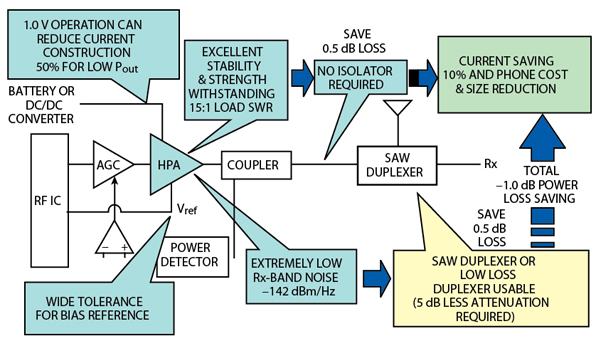
A basic block diagram of a typical amplifier module is shown in Figure 1.
The MOSFET process has many good qualities when applied to CDMA high power amplifiers. MOS devices have excellent stability and ruggedness, characteristics that allow isolator-free operation.

They have an excellent noise figure and produce less RX-band noise, enabling improved receiver sensitivity. Also, they use a simple bias circuit and have a low saturation resistance, a combination that facilitates the design of CDMA phones that operate at lower voltages.1
Isolator-free Systems
In most CDMA systems today, an isolator is inserted between the high power amplifier and the antenna to help attenuate antenna reflections, thereby protecting the amplifier and helping to suppress intermodulation distortion.
Power amplifiers built with the MOSFET process achieve excellent stability under high SWR conditions, so they eliminate the need for an isolator.
This improves the signal budget by approximately 0.5 dB, produces a five percent saving in the current budget and yields a 10 percent saving in power. Eliminating the isolator also saves board space and reduces the cost of the handset.
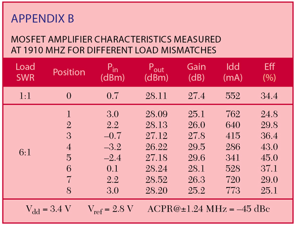
To quantify MOSFET amplifier stability, device measurements were made at the different positions on the Smith chart shown in Figure 2, relating to load SWRs of 1:1 and 6:1. The power amplifiers were operated at Vdd = 3.4 V and Vref = 2.8 V.

The adjacent channel power rejection (ACPR), which was measured at ±885 kHz for the cellular band and at ±1.25 MHz for the PCS band, was maintained at -45 dBc for these upper and lower frequency limits, controlled by varying Pin.
The results for the PCS amplifiers, which are summarized in Appendices A and B, illustrate the consistent performance that CDMA system designers can expect from MOSFET power amplifiers.
MOSFET devices are rugged. They exhibit no degradation when Vdd = 5 V, and they can withstand a 15:1 mismatch with no damage. Figure 3 shows that the MOS design has very good quality and reliability characteristics.
Silicon has 3.3 times better thermal conductivity at 300 K than GaAs, 1.5 W/cm-°C versus 0.46 W/cm-°C, so it dissipates heat faster. Notably, MOSFETs have a negative temperature coefficient, so the power amplifiers do not experience thermal runaway.
Low RX-band Noise
In a CDMA system the TX and RX functions operate simultaneously. Therefore, a duplexer with good rejection and compression characteristics is needed to reduce the RX-band noise coming from the TX output signal.
This necessitates a design tradeoff between the duplexer's size, insertion loss and rejection specification. MOSFET technology eases this tradeoff because it generates less noise than GaAs HBT technology.

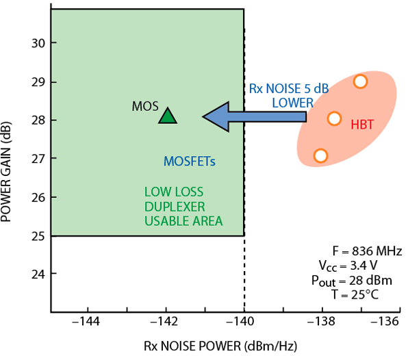
In fact, MOSFET amplifiers achieve 5 dB lower RX-band noise than typical HBT devices, approximately -142 dBm/Hz versus -137 dBm/Hz.
Figure 4 illustrates the RX noise power difference and its beneficial impact on a CDMA system design. The 5 dB improvement in amplifier RX noise level allows the duplexer RX attenuation specifications to be relaxed.
In turn, this enables improved insertion loss characteristics.
These characteristics are shown in Figure 5. Now a lower insertion loss, lower cost duplexer can be used in the system. The saving on the signal budget is approximately 0.5 dB.
This produces another five percent saving in the current budget and achieves another 10 percent saving in power.
High Efficiency
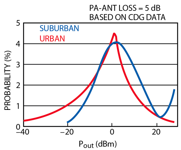
The base station and handset in CDMA systems monitor signal strengths and control the handset's high power amplifier output level accordingly.
Figure 6 shows the standard output power level probability of the high power amplifier measured in urban and suburban conditions. The higher probability output power is found around 0 dBm.

These curves show that to obtain long talk times on batteries, the handset's efficiency at low output power levels is much more important than its efficiency at peak output power.2 A system design that uses a MOSFET amplifier can benefit from this fact.
A well-known technique for improving average system efficiency is to use a bias control system. A key point is that the bias current needed to achieve linearity at the maximum output power level is too large for operating at the smaller output power levels.3
Many adaptive bias control systems are possible. All of them have three important characteristics: small bias control current, gradual control sensitivity and small temperature dependency.
Commonly used bias circuits include the current-mirror and emitter-follower topologies for GaAs HBT amplifiers, and the current-mirror topology for MOSFET devices.
As Figure 7 shows, the current-mirror topology for biasing GaAs HBT power amplifiers requires tens of milliamperes (mA) of control current and has a 6 mA/100 mV control sensitivity and +1000 ppm/°C temperature dependency.
The emitter-follower bias control topology for GaAs HBT devices requires less than 1 mA control current, has 25 mA/100 mV control sensitivity and has +10,000 ppm/°C temperature dependency.

Even better, the current-mirror for biasing MOSFET devices needs less than 1 mA control current and has 4.5 mA/100 mV sensitivity and only +200 ppm/°C temperature dependency.
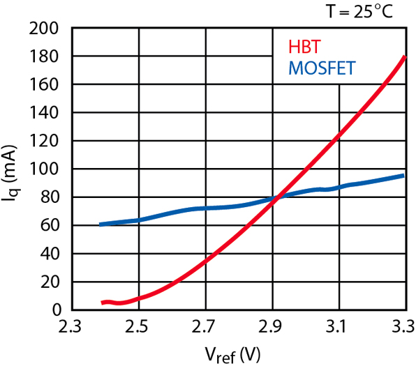
Figure 8 plots the quiescent current (Iq) for MOSFET and HBT devices versus Vref, while Figure 9 shows Iq for these devices versus temperature. In both cases, the superior performance of the MOSFET device is clearly evident.
For discussion purposes, assume a three-step bias control system for Vref for a MOSFET device. It sets Pout < 15 dBm (Iq = 30 mA (Low)), Pout = 15 to 20 dBm (Iq = 50 mA (Mid)) and Pout > 20 dBm (Iq = 100 mA (Hi)).
The operating current (Idd ) versus Pout for this design is shown in Figure 10. Under these conditions, using the probability data, the average current will be approximately 84.6 mA/55 mA (suburban/urban).

Without the bias control system, the average current would be much higher (130.5 mA/109 mA).
Even higher amplifier efficiency can be achieved with a MOSFET device if a voltage (Vdd ) control system is used. This control approach benefits from the MOSFET amplifier's low voltage operation, simple bias circuit implementation and low Ron device characteristics.
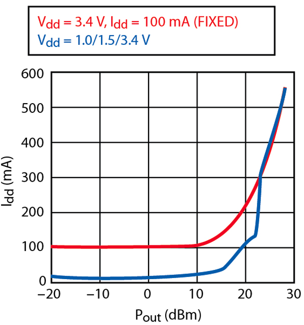
Here the three-step control system sets Pout < 15 dBm (dd = 1 V, Iq = 50 mA (Low)), Pout = 15 to 20 dBm (Vdd = 1.5 V, Iq = 50 mA (Mid)) and Pout > 20 dBm (Vdd = 3.4 V, Iq = 100 mA (Hi)).
Now the average current from the battery is 56.7 mA/32.1 mA (suburban/urban).
Figure 11 shows the gain versus Pout for this voltage control system design and Figure 12 shows the power-added efficiency (PAE) versus Pout data. Figure 13 shows the ACPR vs. Pout data.

The efficiency obtained with a MOSFET amplifier and a Vdd control system is 2.2 to 3.4 times better than it is without a control system. Moreover, it is 1.5 to 1.7 times better than using the bias control method for Vref .
The Vdd control approach also works for Vdd out < 15 dBm output condition. Data for device current (dd ) are plotted in Figure 14.
Figure 15 shows that a MOSFET power amplifier can operate at Vdd = 1.0 V and maintain a +15 dBm output, while meeting the IS-95 specifications for ACPR.
A GaAs HBT device typically needs at least Vdd = 1.6 V to meet these specifications, and usually a few tenths more voltage to account for temperature dependencies.

Designers can take advantage of the MOSFET's low voltage operation to extend battery life by controlling the device voltage to obtain optimal output power.4
One way to implement the Vdd control system is to use a switching DC/DC converter. A key concern regarding this approach is that the converter might add noise to the RX-band.
A test was performed which proved that this was not the case. Figure 16 shows the RX-band noise versus output power with and without the DC/DC converter as the power supply for the MOSFET amplifier.
It demonstrates that there was no measurable addition of noise to the RX-band as a result of using the DC/DC converter.

General Advantages of MOSFET Technology
With the MOSFET process, low cost, large-diameter silicon wafers can be used in manufacturing. Large production quantities of chips are readily obtained.
Also, resistors, capacitors and control devices can be integrated with the RF power transistors, so small-size, low cost MOSFET IC die can be mass produced that reduce the component count of the power amplifier modules.
Figure 17 shows a 6 x 6 mm PCS MOSFET module with a MOSFET IC die and discrete components.
MOSFET power amplifiers have one more characteristic that gives them an edge over other types of amplifiers. Silicon is considered an environmentally compatible material, whereas the GaAs in HBT devices, among others, is not.
This is a consideration for companies interested in environmentally safer products.
Conclusion
The MOSFET process has advanced to the point where it is now a reliable technology for building high power amplifiers for CDMA systems.
Designers can take advantage of MOSFET characteristics to develop more efficient, lower cost handsets. In particular, they can use the silicon technology to create systems with isolator-free operation, low RX-band noise generation for better sensitivity and high efficiency operation.
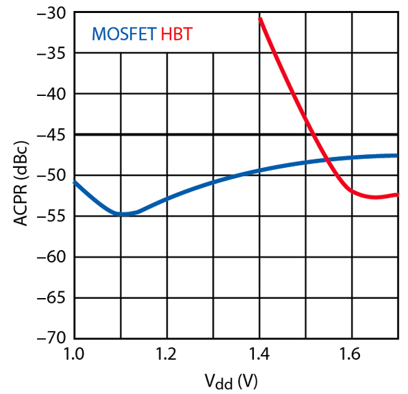
Figure 18 summarizes the advantages of using flexible, stable MOSFET high power amplifiers.
The MOSFET devices now commercially available include IS-95 compliant CDMA high power amplifier modules for 0.8 GHz cellular-band dual-mode CDMA/AMPS and 1.9 GHz PCS CDMA applications.
These modules have a 6 x 6 mm multi-layer ceramic package with a plastic top that is internally matched to 50 Ω. Standard specifications of the modules are Gain = 24dB (min), Pout = 28 dBm, PAE = 32 percent and Rx-band noise = -142 dBm/Hz.
These products can also be used for cdma2000 1X RTT systems.
References

1. I. Yoshida, "2 GHz Si Power MOSFET Technology," 1997 IEEE International Electron Device Meeting Digest, pp. 51-54.
2. CDMA Development Group, "Optional System Performance Tests," August 1, 1998, Rev 2.0, CDG35, pp. 2-3, 2-4.
3. T. Sato, et al., "Intelligent RF Power Module Using Automatic Bias Control (ABC) System for PCS CDMA Applications," 1998 IEEE International Microwave Symposium Digest, pp. 201-204.
4. J. Staudinger, et al., "High Efficiency CDMA RF Power Amplifier Using Dynamic Envelope Tracking Technique," 2000 IEEE International Microwave Symposium Digest, pp. 873-876.
 Tetsuo Sato earned his BS degree in electrical engineering from Iwate University, Iwate, Japan.

He joined the Hitachi Semiconductor & Integrated Circuit Division in 1974, dedicating most of his tenure to leading system and circuit designs of analog and digital mixed signal ICs for wireless applications.
Sato recently transferred to Hitachi Semiconductor (America) to maximize his core competence for the US wireless market. He currently oversees the technical support infrastructure for all semiconductor products for wireless systems.
His areas of product responsibility include wireless transceiver ICs, RF modules and discrete devices. He is a member of both IEEE Solid-State Circuits and the Institute of Electronics Information and Communication Engineers.
 Chris Grigorean earned his BS degree in electrical engineering from the Florida Institute of Technology, Melbourne, FL.
He is currently working on his MBA degree at San Jose State University. He joined Hitachi Semiconductor (America) in June 2001, and currently serves as an application engineer responsible for product testing and technical support for Hitachi's RF products for wireless devices. His areas of expertise include circuit designs of microstrip, stripline, amplifiers, power splitters, couplers, filters and use of various MMICs for subsystem design and system architecture. Prior to joining Hitachi, he worked at SSE Telecom as an electrical engineer and designed a direct conversion RF module and various other RF circuits for the company's new product line. He is a member of the IEEE MTT society.