
By using impedance or admittance inverters, microwave bandpass filters can be designed more conveniently with only one kind of resonator. Theoretically, the inverters have to be frequency independent. However, this is not true for practical cases.
One of the most serious degradations in frequency response of a bandpass filter from the ideal one is due to the frequency-sensitive coupling structures or inverters.1 In practice, many circuits can operate as inverters even if they are not ideal ones. Because of the frequency dependence of the inverters, microwave filters designed with the standard method,1 in which the inverter values are taken only at the center frequency, have to be modified, or optimized using various methods.
L. Young2 offered a bandwidth contraction factor and a deviation of center frequency for direct-coupled cavity filters to predict the change caused by the frequency-dependent coupling structure using design graphs. The theory gives good results for bandwidths in applications of such filter types. R. Levy3 suggested "ideal transformers with frequency-dependent turns ratio'' on both sides of the inverter, which can be used for the design of shunt inductor-coupled bandpass filters. The model of generalized inverters4 gives an easy and more general way to apply the inverter concept to the discontinuity network. A generalized design approach5 using inverter impedances and associated reference planes is a general method to design filters with distributed prototype filters, and considers the junction discontinuity effect itself. However, the frequency-dependent properties of the two transmission lines on both sides of the discontinuity that gives an impedance ratio should be also considered to design filters more exactly.
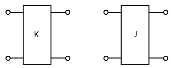
An ideal inverter has a fixed plus or minus 90° phase shift and a parameter K or J analogous to the characteristic impedance or admittance of a transmission line. Practical inverters that are used in standard filter design operate like an ideal inverter at only one center frequency and deviate from ideal performance at frequencies away from it. In this article, practical J inverters are modeled by an ideal J inverter with a frequency-dependent shunt susceptance on each side. In the design process these susceptances can be absorbed into adjacent shunt resonator susceptances to compute improved values for the resonator slope parameters. The case of K inverters is analogous, except that series reactances and series resonators are used.
Typical Inverters
One standard method to design a bandpass filter uses impedance or admittance inverters. The ideal K and J inverters shown in Figure 1 have well-known ABCD matrices given in Equation 1, and have frequency independent characteristics.
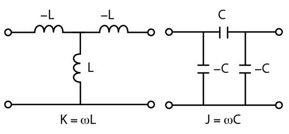

On the other hand, typical inverters have one of three types of frequency dependence: (1) only the real part depends on the frequency (Figure 2 ); (2) only the imaginary part depends on the frequency (Figure 3 ); or (3) both parts depend on the frequency (Figure 4 ).
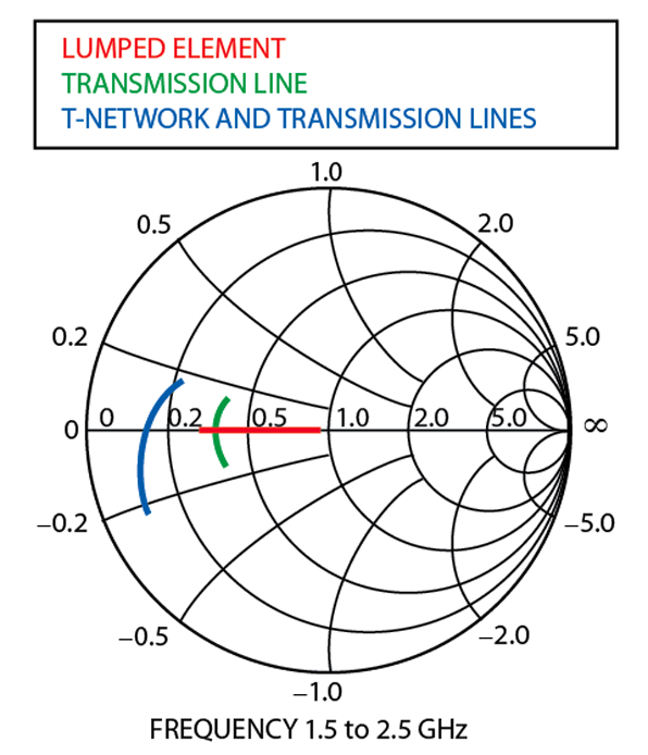
Each inverter can be represented by one port S-parameters on a Smith chart by terminating one port by a constant load of 50 Ω, as shown in Figure 5 .
In the case of the inverter made of lumped elements, only the real part depends on the frequency. This is not serious for filter design, because such frequency dependence of the inverter value does not affect the characteristics of the resonators, and the inverter values and resonator slope parameters change linearly with frequency w as J = ω C and b = ω Cr , hence the coupling coefficients k (k=J/b) remain constant. However, for both the first and the last stages of the bandpass filter, the inverters are not directly applicable but one of the negative elements must be removed, which could introduce small deviation from the theoretical performances.
The inverters of the type (2) and the type (3) have different frequency characteristics from the type (1) inverter. Their immittances change as the frequency varies. Such frequency dependence degrades the filter response because the slope parameters and/or the inverter values do not change linearly as the frequency varies. Such inverter characteristics are discussed theoretically as well as their effect on the performance of the bandpass filters for the transmission line type and the more general type. By comparing the ABCD parameters of the two equivalent circuits, the equivalent values of the transmission line inverter shown in Figures 6 and 7 can be obtained.
The ABCD matrix of an ideal transmission line and that of an ideal inverter with ideal transmission lines or immittances on both sides are given in Equations 2, 3 and 4, respectively.

Comparing Equations 3 and 4 gives the equivalent ideal inverter value, J, and the immittance of transmission line inverter, B, as

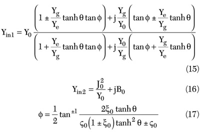
For the first or last stage inverter, another equivalent circuit pair is used. The input admittances Yin1 and Yin2 can be easily obtained using

Comparing these equations J0 and B0 are derived as

The susceptance slope parameters b0 and b for first (or last stage) and mid-stage inverters are determined from B0 and B of Equations 5 and 8, respectively, by using the same definition as a resonator.

where
K = wave number
β = propagation constant
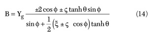
Similarly, equations for the same parameters are derived for an evanescent waveguide inverter shown in Figure 8 . The evanescent waveguide section (length le and characteristic admittance jYe ) with two propagating waveguide sections (length lad or f/2 and characteristic admittance Yg ) is a well-known and widely used inverter. First, the ABCD matrices of (a) and (b) are derived using the equivalent circuit parameters of the waveguide of Figure 9 .


where

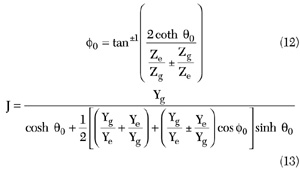
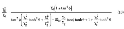
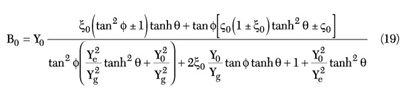
From Equations 11 and 1, the electrical length Φ and inverter value J have to be as Equations 12 and 13 in order to satisfy A=D=0 and the reciprocal condition AD-BC = 1 at center frequency.
Comparing the matrices of Equations 10 and 11 gives the susceptance B as
For the first stage inverter, the input impedances Yin1 and Yin2 in Figure 10 can be also derived and compared. As a result, the inverter value J0 and susceptance B0 are given by
where

The slope parameters for the first (or last) inverters and mid-inverters are calculated as

for the first inverter, and

for mid-inverters (20)
where
Δ = incremental change in the parameters around the center frequency f0
Filter Design Method
By using the inverter analysis of the previous section, bandpass filters can easily be designed with standard design equations modified slightly on the slope parameter β j as

where
β j = bj-1,j + brj + bj,j+1
The parameters brj denotes the slope parameters of the jth resonator, whereas bj-1,j and bj,j+1 are the slope parameters of its adjacent inverters, as shown in Figure 11 . The additional two small slope parameter terms from adjacent inverters are added to the original slope parameter of each resonator. The other processes are the same as the procedure of the conventional standard filter design that uses the concept of inverter with lumped low pass prototype filter.
Design Examples of Bandpass Filters
(A) A Bandpass Filter with Quarter Wavelength Transmission Line Inverter
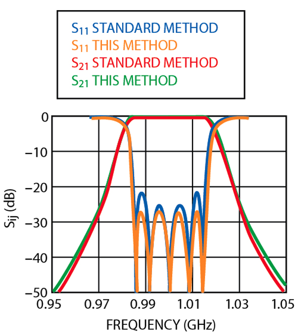
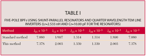
In order to compare the previously described filter design method with the standard one, a bandpass filter was designed with lumped LC resonators and quarter wavelength transmission line inverters using the previous BPF configuration. It is designed for a center frequency of 1.0 GHz, a ripple of 0.01 dB and a fractional bandwidth of 3 percent. The simulated frequency responses are compared in Figure 12 and the designed inverter values are listed in Table 1.
The bandwidths are similar. However, the flat passband ripple is not obtained by the standard method but by the proposed method. Because the loss factors of the resonators and inverters are not considered, the passband ripples can be observed in the return losses, S11 . This method gave the exact bandwidth and passband ripple. In the case of the standard method, the bandwidth was slightly larger than the designed one and the passband ripple was degraded by approximately 5 dB in S11 .
(B) A Bandpass Filter with Evanescent Guide Inverter
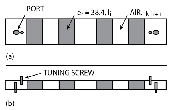
Another design based on the proposed method is a rectangular waveguide bandpass filter with evanescent waveguide inverters,6 as shown in Figure 13 . At 2.59 GHz center frequency, bandpass filters with fractional bandwidths of 2.5 and 10 percent were designed using the same method. A rectangular waveguide (20 by 5mm) and ceramic materials (er =38.4) were used in the filter construction.
To calculate the inverter values, the equations for an inverter using arbitrary elements and transmission lines are used for the standard method, and Equations 13 and 18 are used for the proposed method. The designed parameters are given in Table 2 , in which lKij and li mean the lengths of evanescent sections and dielectric or propagating sections, respectively.
By the standard method, the designed filter response gives too wide a bandwidth (BW = 111 MHz, or result BW vs. wanted BW = 111/65 = 178 percent) and a bad ripple flatness (fluctuation of S11 approximately 2.5 dB), as shown in Figure 14.
On the other hand, the filter designed with this method gives excellent results in bandwidth (exactly 65 MHz) and passband ripples (S11 fluctuation within 0.5 dB).
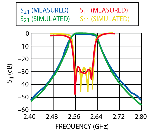
The 2.5 percent bandwidth waveguide filter was designed using this method and the frequency response was measured. The loss terms are not considered in this method. There are no tuning screws in the constructed bandpass filter except at the input and output ports for matching of the transitions from coaxial to waveguide. The measured frequency response agrees well with the expected one except for the insertion loss, as shown in Figure 15.
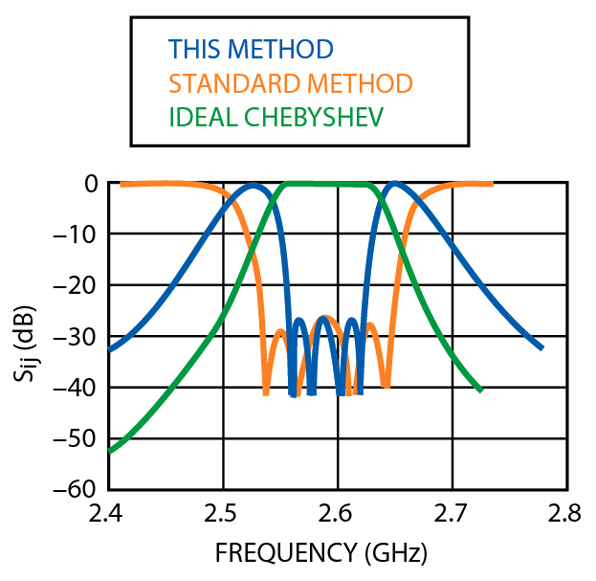
When a filter is designed for a 10 percent bandwidth with 0.01 dB ripple or SWR = 1.1, using this method, the SWR is from 1.10 to 1.07 in a passband, as shown in Figure 16 . The error is only 2.7 percent. The bandwidth error is about 3.5 percent (BW = 250 MHz and 250/259 = 96.5 percent). Therefore, this design method can be used for broader band filter designs.
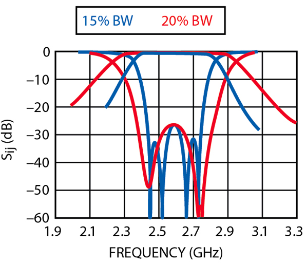
On the other hand, by the conventional standard method, the bandwidth error is about 46.7 percent (BW = 380 MHz and 380/259 = 146.7 percent). For bandwidths of 15 and 20 percent with 0.01 dB ripple, the resultant frequency responses designed by the proposed method show bandwidth errors of only -7.2 and -17.6 percent, respectively, as shown in Figure 17.
Conclusion
One of the most serious factors that degrade the frequency response of bandpass filters designed by the standard method is the frequency dependence of the inverter immittance. In the proposed design method, the immittances of the inverters are considered as part of the adjacent resonators. The frequency-dependent terms of the inverters in the filters are treated as part of the resonator's immittance slope parameters.
These parameters can easily be used to design filters by the conventional standard method with lumped low pass prototype filters. The frequency responses of the filters designed by this method are well matched with ideal Chebyshev responses, without any need for additional optimization or tuning. The proposed method is also applicable to wideband filters design to get better initial design values with ease.
References
1. G. Matthaei, et al., Microwave Filters, Impedance-matching Networks and Coupling Structures, Artech House Inc., Norwood, MA 1980.
2. L. Young, "Direct-coupled Cavity Filters for Wide and Narrow Bandwidths," IEEE Transactions on Microwave Theory and Techniques, Vol. 41, No. 5, May 1963, pp. 162-178.
3. R. Levy, "Theory of Direct-coupled-cavity Filters," IEEE Transactions on Microwave Theory and Techniques, Vol. 15, No. 6, June 1967, pp. 340-348.
4. R. Levy, "A Generalized Design Technique for Practical Distributed Reciprocal Ladder Networks," IEEE Transactions on Microwave Theory and Techniques, Vol. 21, No. 8, August 1973, pp. 519-526.

5. J. Chen, W. Hong and C. Liang, "A New Model of Generalized Invertor and Its Appications," IEEE Transactions on Microwave Theory and Techniques, Vol. 45, No. 1, January 1997, pp.132-135.
6. A. Abdelmonem, J.F. Liang, H.W. Yao and K.A. Zaki, "Full-wave Design of Spurious Free D.R. TE Mode Bandpass Filters," IEEE Transactions on Microwave Theory and Techniques, Vol. 43, No. 4, April 1995.
7. G.F. Craven and C.K. Mok, "The Design of Evanescent Mode Waveguide Bandpass Filters for a Prescribed Insertion Loss Characteristic," IEEE Transactions on Microwave Theory and Techniques, Vol. 9, No. 3, March 1971, pp. 295-308.
8. G.F. Craven and R.F. Skedo, Evanescent Mode Microwave Components, Artech House Inc., Norwood, MA 1987.
Hee Yong Hwang received his BS degrees in biology and electronic engineering from Seoul National University in 1988 and 1992, respectively, and his MS and PhD degrees in electronic engineering from Sogang University in 1995 and 1999, respectively. From March 2000 to February 2001, he was a professor in the department of electronic engineering at Sogang University. He is currently a visiting researcher with the department of ECE, University of Maryland, College Park, MD. He is also a research adviser for Amotech Co. His research interests include microwave passive and active filters, and RF systems.
Sang-won Yun received his BS and MS degrees in electronic engineering from Seoul National University in 1977 and 1979, respectively, and his PhD degree in electrical engineering from the University of Texas at Austin in 1984. Since September 1984, he has been with the department of electronics engineering at Sogang University, where he is a full professor. He has been the Korea MTT chapter chairman since January 1999. His research interests include microwave and millimeter-wave devices and circuits.