
During the past decade, there has been significant progress in monolithic power amplifiers operating at RF and microwave frequencies over narrow and broadbands for both commercial and military applications.

For numerous applications, including handsets, VSAT and transmit/receive modules, these amplifiers are produced in large quantities using MESFET, HBT and PHEMT technologies.1-12 Table 1 summarizes the performance of C-band MMIC power amplifiers. Several packaging technologies are being employed including plastic, ceramic and carrier mounting to develop cost-effective MMIC-based power amplifier products. MMIC power amplifiers have many potential advantages as compared to internally matched power amplifiers. They include compact size and lightweight, lower parts count, higher reliability and lower cost. The devices are usually in one chip or package instead of several packages. Multi-stage designs have higher gain (20 to 30 dB). No external series DC block capacitors at the input and output are required. Most of the time, no external 50 to 100 pF capacitors are needed and no external biasing chokes are required. Also, no additional design or tuning is required and higher overall PAE is achieved. Under backoff, the degradation in PAE is lower. A dynamic range of about 8 dB, over which the PAE remains almost constant, can be achieved.
The 2.5 W broadband MMIC power amplifier was developed using a multi-function self-aligned gate (MSAG) MESFET process3-7 used to fabricate low cost, high volume, high performance and highly reliable multi-function monolithic ICs. Because of its versatility in fabricating both low noise and power MMICs and high speed large scale integration (LSI) circuits on a single chip, this process has been named the multi-function self-aligned gate process. The MSAG process has eliminated the need for a gate recess, the single most important yield and reproducibility limiting step. The process requires an additional mask for each implant, which may include an enhancement-mode FET (EFET), a depletion-mode FET (DFET), a low noise FET, a switching FET, a power FET and 'n' implants. Each implant is optimized for its respective function. The process is available as a standard foundry service to outside users.

This article describes the design, fabrication and test results of a fully monolithic, class AB, 2.5 W broadband, two-stage power amplifier with over 45 percent PAE. In addition to power output, gain and PAE as a function of input power and drain-source voltage, data on input SWR, second- and third-harmonic generation, noise figure and third-order intercept (TOI) are included. The primary goal of this project was to develop a generic two-stage 0.3 to 3.0 W power amplifier chip which operates from 3 to 10 V drain voltage and provides excellent PAE even under 5 to 8 dB backoff power. Both chip and packaged die data are provided.
FET Design and Performance

The FET used in the MMIC power amplifier has a 625 µm gate periphery, six fingers and 20 mm gate-to-gate spacing to obtain maximum gain while meeting thermal requirements. This device em- ploys two, plated-through, source vias for low inductance source grounding and good heat sinking. The 0.4 mm gate length MSAG FET features outstanding performance along with remarkable robustness to burnout. The FET equivalent circuit model is shown in Figure 1 . Table 2 provides the equivalent circuit parameter values of a 625 µm gate periphery FET, biased at several bias conditions. A user-defined nonlinear model for this FET was developed based on pulsed I-V characteristics and S-parameters measured over a wide range of bias voltages. The nonlinear model has been validated using load-pull data and single-stage hybrid amplifier test data. The typical measured performance for the 0.625 mm FET biased at 10 V and 25 percent IDSS , tested in a hybrid amplifier configuration at fo = 14.5 GHz, is Po = 27 dBm, PAE = 60 percent and associated gain = 8 dB.
The measured load for this FET for high PAE applications is equivalent to a parallel combination of a resistor and a capacitor of 85 Ω and -0.19 pF, respectively. At C-band, the maximum available power gain is approximately 13 to 14 dB.
2 W MMIC Amplifier Design
MMIC power amplifier design techniques are constantly being improved by using new topologies, nonlinear device models, EM simulations, new devices and low loss inductors. Accurate simulations, a repeatable process and statistical analysis play a significant role in the development of MMIC power amplifier chips in a single pass. Small- signal simulators do a good job in terms of input match and gain, but are not adequate to simulate power performance. Nonlinear simulators and/or extensive source-pull and load-pull data are required to design high efficiency and wider-bandwidth MMIC power amplifiers.
The bias point of the amplifier was selected for class AB operation (25 percent Idss ) of the device in order to obtain the best compromise of power output, gain, PAE, linearity and variable power supply operation over the C-band. The power output goal for the IC was 2.5 W. Based on the output matching network's dissipative and mismatch loss, and 0.8 W/mm power output density at VDS = 8 V for the FETs, a total of 5 mm gate periphery was selected for the output stage FETs. The first stage uses two 0.625 mm gate periphery FETs, resulting in a FET aspect ratio of 1:4. The FET aspect ratio of 1:4 was chosen to offer the best compromise between the PAE and linearity, and to maintain good RF performance of the amplifier over a large drain voltage range as well as under backoff power conditions.

Traditionally, a power amplifier can be designed based on the loadline method.13-15 The design of the two-stage broadband MMIC power amplifier was based on a methodology using small-signal and nonlinear FET models, and load-pull data obtained at the operating bias point. In this method, the loadline technique is used initially to optimize the circuit parameters. The optimum load impedances ZL1 and ZL2 at the drain of the first and second stage FETs, respectively, needed to realize maximum output power and PAE, are shown in Figure 2 . Then the design is simulated using a nonlinear model to calculate the power compression of each stage, and the output power and PAE as a function of input power. Since it is very difficult to realize the required load impedances over wide bandwidths and to optimize a circuit using a nonlinear model, the above design process is repeated so that an optimum solution, for simultaneous match for load impedances at the drain of each FET and best gain, power and PAE, is achieved.

In the IC design a binary matching scheme was used employing low pass networks, as shown in Figure 3 . Both lumped and distributed circuit elements were used in the impedance matching networks. No attempt was made to realize a compact size. Low pass matching sections consisting of series high impedance lines and metal-insulator-metal (MIM) capacitors in shunt were used. Since the FET's input impedance is lower than the output impedance, more matching elements were used in the input and interstage to match the device impedance for maximum gain, Po and PAE.
The input stage, which has a limited gain compensation network, was designed for good input match as well as for maximum power transfer at the high frequency end. The interstage matching network was designed to provide a flat gain response and enough output power to the output stage FETs for achieving maximum output power and PAE. The output matching elements were selected to provide an optimum load match with minimum possible insertion loss, since the efficiency is reduced to a greater extent by a given amount of loss due to decreased power output, gain and available DC power at the FET drain pads.

Both stages, as well as the complete amplifier, were designed to be unconditionally stable over 3 to 10 V drain power supply voltage and 25 to 50 percent Idss drain current. Experience has shown that, for MSAG FETs, the standard even-mode (K>1) and odd-mode stability analyses are adequate to avoid microwave oscillations. However, under large-signal condition and pulsed operation, it is necessary to use a worst-case K-factor greater than 1, when S-parameter data is used for various bias conditions from Vds = 3 V and 50 percent Idss to Vds = 10 V and 25 percent Idss . This approximately replicates the envelope a full cycle of the input signal experiences during the large-signal and pulsed operation. Imposing a K>2.0 condition for Vds = 10 V and 25 percent Idss small-signal S-parameters was found to be necessary to ensure K >1 under all conditions.
Electromigration requirements dictate the microstrip and inductor line widths carrying the DC current. A very conservative current density of 2.2 x 10⁵ A/cm2 was used as an electromigration limit for the 4.5 µm thick gold conductors. This translates to a maximum allowed current per unit line width of 10 mA/µm. Special care was exercised to maintain the symmetry in the amplifier layout and isolation resistors were used to prevent odd-mode or loop oscillations. Table 3 summarizes the design parameter values of the two-stage 2.5 W power amplifier chip shown in Figure 4 . The chip size is 3.4 x 4.4 mm.

Circuit Fabrication
The 2.5 W power amplifier chip was fabricated using the ion-implanted, planar refractory gate, MESFET MMIC process MSAG,5 which features a full suite of active and passive components fabricated on 4" diameter GaAs wafers. The devices were fabricated using the Process 5A implant. The process includes Au/Ge/Ni metallization for ohmic contacts and 0.4 µm TiWN Schottky barrier gates, along with thin film and ion-implanted resistors. The 0.4 µm TiWN gates are covered by a 0.8 µm overlay after planarization. The MSAG TiWN gate is extremely robust (it survives a 900°C rapid thermal anneal temperature), which results in an MTTF of 100 years at a channel temperature of 150°C. A thickness of 2000 Å silicon nitride (ε r = 6.8) is used for both MIM capacitors and passivation. The air bridges, microstrip lines and bonding pads are 4.5 µm thick plated gold. The standard MSAG process also uses two layers of polyimide (ε r = 3.2), interlevel dielectric (3 µm thick) for crossovers and a scratch protection layer (7 µm thick) for mechanical protection of the finished circuitry. The substrate thickness of the amplifier chip is 75 µm.
Test Data

The C-band MMIC amplifier chips were tested using standard carriers as well as in commercial ceramic packages. Several 2.5 W amplifier chips were assembled on gold-plated CuW carriers for RF characterization. The CuW material was chosen for its good thermal conductivity and good thermal expansion match to GaAs and alumina. The ICs were die attached using gold-tin (AuSn) at 300°C on a pedestal in order to keep bond wire lengths to a minimum, between the chip and the input and output microstrip lines which were printed on 15 mil alumina substrate. They were characterized for power output and PAE as a function of frequency at the nominal bias conditions. They were also tested over a large range of drain voltages at the center frequency. Both second- and third-harmonic power levels were measured at the fundamental frequencies of 5.5 and 7.0 GHz.
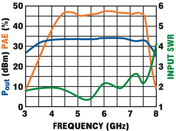
Typical CW measured Pout and PAE for MMIC chips on CuW carriers at Vds = 10 V and Pin = 18 dBm, and simulated performance, is compared in Figure 5 . The agreement between the measured and simulated performance, over most of the frequency range, is quite good. Typical CW measured Pout , PAE and input SWR at Vds = 8 V, Idq = 360 mA and Pin = 18 dBm are shown in Figure 6 as a function of frequency.The amplifier has greater than 34 dBm power output, 16 dB gain and better than 45 percent PAE over the 4.5 to 7.4 GHz frequency range.
A plot of output power and PAE as a function of input power at 5.5 GHz is shown in Figure 7 . Figure 8 depicts the power output and PAE as a function of drain voltage VDS at Idq = 360 mA, Pin = 18 dBm and f = 5.5 GHz.

This plot shows that these chips exhibit more than 45 percent PAE over a large range of drain bias voltages (4 to 9 V) and the output power is approximately linear with drain voltage from 3 to 10 V.
No oscillations were observed when the chips were biased from 3 to 10 V. As shown in Figure 9 , the typical measured second- and third-harmonic levels at Vds = 8 V and Pin = 18 dBm were below -25 dBc and -28 dBc.
Typical measured noise figure and output third-order intercept point values over the 4.5 to 7.1 GHz frequency range were 8.8 dB and 43 dBm, respectively. All non-harmonically related outputs were below -70 dBc for Pin = 5 to 20 dBm, Vds = 3 to 10 V and load SWR = 3. The thermal resistance measured between the die and the carrier is 16°C/W.

The C-band chips were assembled and tested in commercially available ceramic packages having a CuW base. The devices were mounted using AuSn solder.
Typical measured characteristics for the packaged ICs are plotted in Figures 10 through 13, and the package Po and PAE data is slightly lower than the carrier mounted data due to package leadframe parasitics. The NF, TOI, stability and thermal resistance values were similar for both cases.
References

1. H.Q. Tserng and P. Saunier, "Advances in Power MMIC Amplifier Technology in Space Communications," SPIE-Monolithic Microwave Integrated Circuits for Sensors, Radar and Communications Systems Proceedings, 1991, pp. 74-85.
2. D. Willems and I.J. Bahl, "Advances in Monolithic Microwave and Millimeter-wave Integrated Circuits," IEEE International Circuits and Systems Symposium Digest , 1992, pp. 783-786.
3. A.E. Geissberger, R.A. Sadler, M.L. Balzan and J.W. Crites, "TiW Nitride Thermally Stable Schottky Contacts to GaAs: Characterization and Applications to SAG FET Fabrication," J. Vacuum Science Technology , Vol. B5, 1987.
4. A.E. Geissberger, R.A. Sadler, E.L. Griffin, I.J. Bahl and M.L. Balzan, "Refractory Self-aligned Gate Technology for GaAs Microwave FETs and MMICs," Electronics Letters , Vol. 23, Sept. 1987, pp. 1073-1075.

5. A.E. Geissberger, I.J. Bahl, E.L. Griffin and R.A. Sadler, "A New Refractory Self-aligned Gate Technology for GaAs Microwave Power FETs and MMICs," IEEE Transaction Electron Devices , Vol. 35, May 1988, pp. 615-622.
6. A.E. Geissberger, et al., "Fabrication, RF Performance and Yield of a Combined Limiting Amplifier and Dual-modulus Prescaler GaAs IC Chip," IEEE Transactions on Microwave Theory and Techniques , Vol. 36, December 1988, pp. 1706-1713.
7. W.L. Pribble and E.L. Griffin, "An Ion-implanted 13 Watt C-band MMIC with 60 Percent Peak Power Added Efficiency," IEEE Microwave and Millimeter-wave Monolithic Circuits Symposium Digest , 1996, pp. 25-28.
8. J.P. Fraysse, et al., "A 2 W, High Efficiency, 2-8 GHz, Cascode HBT MMIC Power Distributed Amplifier," IEEE MTT-S International Microwave Symposium Digest , 2000, pp. 529-532.

9. S.L.G. Chu, et al., "A 7.4 to 8.4 GHz High Efficiency PHEMT Three-stage Power Amplifier," IEEE MTT-S International Microwave Symposium Digest , 2000, pp. 947-950.
10. Y.F. Wu, et al., "3-9 GHz GaN-based Microwave Power Amplifiers with L-C-R Broadband Matching," IEEE Microwave and Guided Wave Letters , Vol. 9, August 1999, pp. 314-316.
11. M.R. DeHaan, et al., "A 15 W Dual Band HBT MMIC Power Amplifier," IEEE MTT-S International Microwave Symposium Digest , 1997, pp. 1425-1427.
12. P.M. White and T.M. O'Leary, "A 50 Percent Efficiency 8-watt C-band PHEMT Power MMIC Amplifier," IEEE GaAs IC Symposium Digest , 1995, pp. 277-279.
13. S.C. Cripps, RF Power Amplifiers for Wireless Communications , Artech House Inc., Norwood, MA 1999.

14. E.L. Griffin, "Application of Loadline Simulation to Microwave High Power Amplifiers," IEEE Microwave Magazine , Vol. 1, June 2000, pp. 58-66.
15. K. Chang, I.J. Bahl and V. Nair, RF and Microwave Circuit and Component Design for Wireless Systems , John Wiley & Sons Inc., New York, NY 2002, Chapter 11.
 Inder J. Bahl received his BS degree in physics from Punjab University, India, in 1965, his MS degree in physics and his MS (Tech.) in electronics engineering from Birla Institute of Technology and Science, Pilani, India, in 1967 and 1969, respectively. In 1975, he received his PhD in electrical engineering from the Indian Institute of Technology, Kanpur, India.

From 1969 to 1981, Dr. Bahl did research in parametric amplifiers, PIN diode phase shifters, microwave and millimeter-wave integrated circuits, printed antennas, phased array antennas, millimeter-wave antennas, and medical and industrial applications of microwaves. He joined the ITT Gallium Arsenide Technology Center in 1981.
His current interests are in the areas of device modelling, high efficiency, high power amplifiers, 3-D MMICs, and the development of MMIC products for commercial and military applications.