
As a newcomer in the mature Silicon world, Gallium Nitride has been undoubtedly one of the groundbreaking technologies of the RF industry. Long considered as a very high end and high cost technology targeted at military applications, GaN made its entrance in Huawei’s fourth generation (4G) Long-Term Evolution (LTE) Remote Radiohead (RRH) base stations in mid-2010s. After that, GaN RF devices witnessed significant market adoption in commercial telecom infrastructure applications owing to their high power density and smaller form factor. Following the deployment of higher frequencies in sub-6 GHz 5G bands, GaN demonstrated properties that exceed the existing Silicon based LMDOS technology in terms of higher bandwidth and higher power density requirements. With the emerging market opportunities, the following questions are being raised in the industry: What is the business outlook for the GaN RF market with the arrival of 5G? Which technology, GaN-on-Silicon Carbide (SiC) or GaN-on-Silicon, will more successfully grow its market? Which business models will dominate in the market? How will the GaN RF business evolve in view of the US-China tension, which is becoming more sensitive than ever?
GaN-based Military: Faster, Better, Stronger!
National security has always been one of the top priorities for any country. Thus, a significant portion of the national budget is reserved for military expenditure. In the search for faster, better, and stronger defense and attack strategies, military applications prioritize high-performance systems. Hence, faster and higher quality data communication offering better military intelligence, or conversely jamming capability to create an advantage in a conflict have been crucial for military organizations. Over the couple of decades, investments and development of next-generation electronic systems resulted in deployment of solid-state technologies, especially in military radar, electronic warfare, and military communications. In the domain of military radar, Active Electronically Scanned Array (AESA) systems replaced the old vacuum tubes, enabling several advantages such as larger detection area, faster scanning rates and higher spatial resolution as well as scalability and easier configuration of transceivers. In this context, using GaN-on-SiC in AESA technology helps to reduce the footprint and weight while increasing the system efficiency. As an alternative to LDMOS and GaAs, GaN achieves high power density and higher power added efficiency with high thermal conductivity while fitting in size-constrained spaces.
Over the last years, GaN deployment in military radar has become extremely popular with long running and high-budget projects in several countries. Following the USA, which is leading in GaN based radar implementation, Europe, Korea and China have also set up numerous projects in order to leverage GaN systems’ higher performance, scalability, and small size.
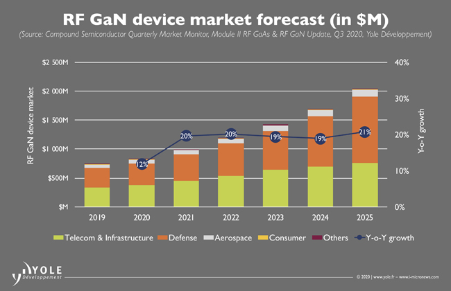
For this reason, GaN RF devices for military use is expected to increase rapidly and the value is expected to exceed US$1 billion by 2025 (See Figure 1)[1]. According to Yole Développement (Yole), the high number of GaN devices in AESA radar represents an interesting market opportunity for military foundries and contractors. While high cost is still considered as the main bottleneck for GaN, the defense industry expects cost reduction with the adoption of GaN in commercial markets, especially in the 4G and 5G telecom infrastructure segment.
5G Telecom Infrastructure: GaN is setting the rules
In the dynamic 5G infrastructure market, there is a continuous race for more efficient antenna types. Switching technology from RRH to Active Antenna Systems (AAS) will transform the RF front ends from a low number of high-power RF lines to a large number of low-power RF lines. Meanwhile, deployment of higher frequencies in the sub-6 GHz as well as in the mm-wave regimes, push OEMs to look for new antenna technology platforms with larger bandwidth, higher efficiency, and better thermal management. In this context, GaN technology has become a serious competitor to LDMOS and GaAs in RF power applications, showing continuous performance and reliability improvement leading, potentially, to a lower cost at the system level. Following its penetration into the 4G LTE telecom infrastructure market, GaN-on-SiC is expected to maintain its strong position in 5G sub-6 GHz RRH implementations. However, in the emerging segment of 5G sub-6 GHz AAS - massive multiple input and multiple output (MIMO) deployments - the rivalry between GaN and LDMOS continues. While cost-efficient LDMOS technology carries on with noteworthy progress in high-frequency performance for sub-6 GHz, GaN-on-SiC offers remarkable bandwidth, PAE, and power output. Indeed, following the China Unicom and Telecom merger requiring >150 MHz bandwidth, GaN technology has been chosen for AAS. 5G telecom infrastructure is a very dynamic market requiring significant strategic decisions from OEMs, which could create new opportunities for GaN technology platforms.
Regarding the small cells, they started entering the market initially in the mm-wave regime to address the demand in the dense urban areas. These systems are poised to grow rapidly, especially owing to their small size and the need for multiple devices because of their short range. In this emerging segment, GaN-on-SiC and GaN-on-Si solutions are being considered amongst potential candidates, together with SiGe, SOI, CMOS and GaAs. The GaN industry has already started to launch products targeting these applications with innovative integration techniques.
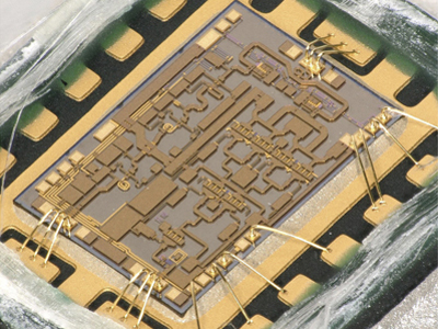
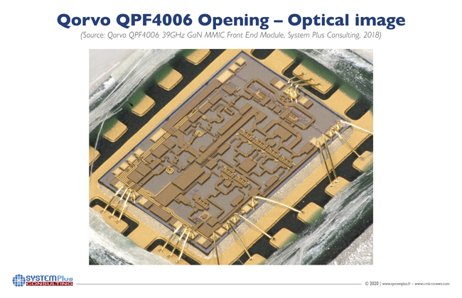
As analyzed by System Plus Consulting, Qorvo has been one of the first companies to offer an integrated GaN-on-SiC solution addressing the mm-wave segment. With a front-end module approach, Qorvo’s product includes multi-function GaN MMICs with 0.15 micron GaN-on-SiC technology, with targeted operating frequency between 37-40.5 GHz (see Figure 2)[2]
Integration capability is indeed a key asset in the RF industry. Space saving and RF loss reduction are the main drivers for device integration. Offering both high power density and low noise characteristics, GaN technology enables monolithic and efficient integration of power amplifiers (PA), low-noise amplifiers (LNA), and the switch technologies on both SiC and Si substrates. In this context, GaN-on-Si technology stands as a potential challenger to GaN-on-SiC and can promise cost-efficient integrated solutions with low cost and large diameter Silicon substrates, as well as a scalable substrate supply chain. As of Q3-20, even though the GaN-on-Si market volume for telecom infrastructure remains tiny, technology developments at sub-6 GHz and mmWave bands are closely followed and evaluated by telecom equipment vendors.
Nonetheless, the GaN RF business is not only dependent on OEM technological choices, but also on the geopolitical context. However, following USA’s sanctions related to Huawei in Q2-2019, a short supply situation occurred in 2019, mainly in the GaN-based telecom infrastructure market. As a result, it will be important to watch how various strategic partnerships and investments unfold during the coming years.
5G Handset PA: GaAs or GaN?
The 5G telecom infrastructure market is not the only opportunity for a GaN-on-Silicon technology platform. Over the last years, several companies have been seriously developing PA technology for the 5G handset market. Driven by the desire of OEMs to save space in RF front ends in handsets, GaN could bring its high-power density and high efficiency benefits and revolutionize the RF industry. As a newcomer, GaN faces strong competition from its III-V cousin GaAs in the Sub-6 GHz and mmWave domains. As a main building block of the 3G and 4G handset PA, GaAs will continue its significant deployment in sub-6 GHz phones, as it meets the stringent requirements for linearity and power. Each generation of phones has required more bands and more PAs, and with the transition to 5G, Yole expects an increase in the total PA size per phone. For mobile connectivity, the trend is moving to an SiGe-based System-on-Chip (SoC) solution, except for high-end phones where GaAs PA remains due to better performance. However, the newly released Wi-Fi 6E standard will go to 6 GHz where SiGe performance will be limited and GaAs adoption is favorable.
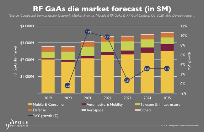
In summary, the GaAs RF die market driven by the high-volume handset market is expected to grow to beyond US$3.6 billion by 2025, as forecast in Yole’s Compound Semiconductor Monitor Service Q3-2020 update. This includes a quarterly update on RF GaN and RF GaAs markets and provides an overview on the competition between possible technology platforms for sub-6 GHz and mmWave RFFE architecture (see Figure 3). However, similar to the GaN RF market, even the mature GaAs RF industry has felt the impact of the US-China trade tension and pandemic outbreak, which created different dynamics in the global smartphone market in the 2019-2020 period.
To sum up, RF GaN business outlook is bright but not straight forward. Facing the “moving target” of mature Silicon and GaAs technology platforms in 5G infrastructure and RFFE, the GaN industry is evolving and winning new battles each day. Looking into the future, GaN has indeed exciting business opportunities in the high-volume commercial markets. Now the question is which OEM will shape its future, and when?
System Plus Consulting and Yole will continue their investigations and invite you to follow them all year long with more analyses, articles, and interviews.
 Bio:
Bio:
As a Technology & Market Analyst, Compound Semiconductors, Ezgi Dogmus, PhD, is a member of the Power & Wireless division at Yole Développement (Yole). She contributes daily to the development of the activities of the division with a dedicated collection of market & technology reports as well as custom consulting projects. Prior to Yole, Ezgi was deeply involved in the development of GaN-based solutions at IEMN (Lille, France). Ezgi also participated in numerous international conferences and has authored or co-authored more than 12 papers. Upon graduating from University of Augsburg (Germany) and Grenoble Institute of Technology (France), Ezgi received her PhD in Microelectronics at IEMN (France).
This article was written in collaboration with Ahmed Ben Slimane, Technology & Market Analyst, Compound Semiconductor Monitors from Yole Développement (Yole) and Elena Barbarini, Semiconductor Devices Department Director from System Plus Consulting.