
Technical Feature
A 2.4 GHz Polarization-diversity Planar Printed Dipole Antenna for WLAN and Wireless Communication Applications
This article presents the design simulation, fabrication and measured performance of a 2.4 GHz polarization-diversity printed dipole antenna for wireless communication applications. Two orthogonal printed dipole antennas, each with a microstrip via-hole balun for vertical and horizontal polarization, are combined and fabricated on a PCB substrate. PIN diodes are used as switches to select the desired antenna polarization. The 3D finite-element-method (FEM) electromagnetic EM simulator, HFSS, is used in the design simulation of this planar antenna structure. Numerical and measured results of the antenna radiation characteristics, including input SWR, radiation pattern coverage and polarization-diversity, are presented and compared.
Huey-Ru Chuang, Liang-Chen Kuo, Chi-Chang Lin and Wen-Tzu Chen
National Cheng Kung University, Tainan, Taiwan
In wireless communication systems, such as wireless local area networks (WLAN), research and development efforts are aiming at smaller size and better performance. In addition to the use of signal processing techniques to improve communication channel capacity, the radiation characteristics of the portable antenna system is also very important for communication performance.
In urban or indoor environments, the radio wave will propagate through complicated reflection or scattering processes. The polarization of the radio wave may change significantly. In order to effectively receive the communications signal, a polarization-diversity antenna for wireless communications may become an important requirement. A polarization-diversity antenna may have a pair of linearly-polarized antennas, and the radio signal received on both antenna is sampled and compared at certain time intervals. Then the antenna with the best signal quality is selected.

Fig. 1 A 2.4 GHz polarization-diversity antenna.
A typical dipole antenna radiates a vertically polarized EM wave and has an omnidirectional antenna pattern. In order to have a preferred planar antenna structure for this 2.4 GHz polarization-diversity antenna, a printed dipole antenna with a microstrip via-hole balun is designed. As shown in Figure 1 , two orthogonal printed dipole antennas, for vertical and horizontal polarization, respectively, are combined and fabricated on a PCB substrate. PIN diodes are used to switch and select the desired antenna polarization.
In the antenna design, the high frequency structure simulator (HFSS), based on a 3D FEM, was employed for design simulation of the complete printed dipole structure. A printed dipole antenna and a polarization-diversity planar dipole antenna board (with a polarization-selection PIN diode circuit) have been fabricated on FR-4 PCB substrates. A complete 3D structure FEM simulation and the measured performance of the realized printed dipole-antenna are compared. The measured radiation characteristics of the polarization-diversity planar dipole antenna, including input SWR, radiation pattern coverage and polarization diversity, are presented.

Fig. 2 Printed dipole antenna with a microstrip balun.
Printed Dipole Antenna with Microstrip Balun
As shown in Figure 2 , a printed dipole antenna has a printed microstrip balun which acts as an unbalanced-to-balanced transformer from the feed coaxial line to the two printed dipole strips. The length of the dipole strip and the balun microstrip are both about 1/4 wavelength. The ground plane of the microstrip line and the dipole antenna strips are in the same plane. A via-hole permits the feed point 2 of a printed dipole strip to have the same phase as the feed point 1 of the other printed dipole strip. Due to the 180° phase difference between the top strip and the ground plane of the microstrip line, the feed point 2 of the printed dipole strip will have 180° phase difference with the other feed point 1. Accurate dimensions of the printed dipole strip and the microstrip balun structure are determined by numerical simulation, using HFSS.

Fig. 3 Simulated performance of a 2.4 GHz printed dipole antenna placed horizontally; (a) input SWR, (b) E-plane pattern and (c) H-plane pattern.
The simulation results for a 2.4 GHz printed dipole antenna placed horizontally with a microstrip via-hole balun and fabricated on an FR-4 substrate are shown in Figure 3 . The input SWR is less than 1.5 from 2.2 to 2.6 GHz. The simulated E- and H-plane antenna patterns are very close to those of an ideal dipole antenna, where the H-plane pattern is omnidirectional. Figure 4 is a photograph of a realized antenna. The measured input SWR and antenna patterns (measured with the dipole placed vertically) agree well with the simulation results, as shown in Figure 5 .

Fig. 4 A 2.4 GHz printed dipole antenna with a microstrip via-hole balun; (a) top view and (b) bottom view.
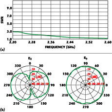
Fig. 5 Measured input SWR (a) and radiation patterns (b).
Planar Polarization-diversity Printed Dipole Antenna
Figure 6 shows photographs of a realized 2.4 GHz planar polarization-diversity antenna consisting of two orthogonal printed dipole antennas with a polarization-switched PIN diode circuit. Each printed dipole has a microstrip via-hole balun. The terminals of the two baluns are connected to a PIN diode selection circuit. Voltages from the transceiver circuit (±5.0V) are fed through a cable to the input of the PIN diode circuit section, to short or open-circuit the PIN diodes. Hence, either the vertical or horizontal printed dipole can be selected and connected to the transceiver.
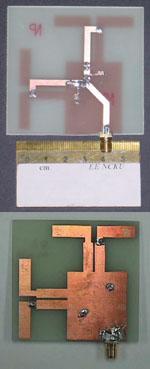
Fig. 6 A 2.4 GHz planar polarization-diversity antenna with a polarization-switched PIN diode circuit; (a) top view and (b) bottom view.
Since the two dipoles are very close to each other and near the PIN diode circuit section, EM coupling will degrade the performance of each dipole. Figure 7 shows the input SWR simulation results with the vertical dipole antenna selected (+5V to PIN diode switching circuit). The input SWR is less than 2 from 2.25 to 2.60 GHz. The simulated E- and H-plane antenna patterns are all very close to those of an ideal dipole antenna, of which the H-plane pattern is still omnidirectional, as shown in Figure 8 . Note that the dominant polarization is the vertical (E ) field, which agrees with the selection of the vertical dipole. The antenna pattern has some attenuation in the direction of the PIN diode circuit board. It can also be seen that a certain level of the input RF signal is induced to the horizontal antenna path by EM coupling, which generates some level of cross-polarization field. Figure 9 shows the simulation results with the horizontal dipole antenna selected (-5V to PIN diode switching circuit). Results similar to the ones obtained for the vertical dipole antenna can be observed, except that the dominant polarization is the horizontal (E
 ) field, which agrees with the selection of the horizontal dipole.

Fig. 7 Input SWR simulation of a 2.5 GHz polarization-diversity dipole antenna with the vertical dipole selected.

Fig. 8 Simulation of a 2.5 GHz polarization-diversity dipole antenna with the vertical dipole selected; (a) E -field E-plane pattern, (b) E -field H-plane pattern, (c) E -field (cross-polarization ) E-plane pattern and (d) E -field (cross-polarization) H-plane pattern.

Fig. 9 Simulation of a 2.4 GHz polarization-diversity printed dipole antenna (with the horizontal dipole selected); (a) input SWR, (b) E -field E-plane pattern, (c) E -field H-plane pattern, (d) E -field (cross-polarization ) E-plane pattern and (e) E -field (cross-polarization) H-plane pattern.
The measured antenna input SWR with vertical or horizontal dipole selection confirms the input SWR of each dipole antenna (through the PIN diode selection circuit) is less than 1.5 from 2.2 to 2.6 GHz, which agrees with the HFSS simulation results. The measured antenna patterns with the selection of the vertical or horizontal dipole shows that for the selection of the vertical dipole, the H-plane pattern is still quite omnidirectional (as an ideal vertical dipole) with some attenuation in the direction of the PIN diode circuit board. Figures 10 and 11 show the mesured SWR and antenna patterns, respectively. A certain level of the induced cross-polarization pattern is observed as predicted by the HFSS simulation due to the proximity of the horizontal dipole strip and the PIN diode circuit board. As for the selection of the horizontal dipole, the E-plane pattern is also close to that of an ideal horizontal dipole. Also, the induced cross-polarization pattern is observed, which is the same situation as the selection of the vertical dipole. The measured data shows a good agreement with the HFSS simulation results and how the antenna polarization-diversity is working.

Fig. 10 Measured input SWR of a 2.4 GHz polarization-diversity printed dipole antenna; (a) vertical dipole selection and (b) horizontal dipole section.

Fig. 11 Measured co- and cross-polarized patterns of a 2.4 GHz polarization-diversity printed dipole antenna; (a) vertical dipole selected and (b) horizontal dipole selected.
Conclusion
3D FEM design simulation, realization and measurements of a 2.4 GHz printed dipole antenna (with a microstrip via-hole balun) and a planar polarization-diversity printed dipole antenna are presented. The planar polarization-diversity antenna consists of two orthogonal printed dipole antennas for vertical and horizontal polarization and is fabricated on a FR-4 PCB board. A PIN diode switching circuit is used to select the desired antenna polarization. Satisfactory agreement between simulation and measurements is observed. The measured input SWR of the realized printed dipole antenna is less than 1.5 from 2.2 to 2.6 GHz. The measured input SWR of the vertical and horizontal dipole (through the PIN diode switching circuit) of the realized planar polarization-diversity antenna is less than 1.5 from 2.3 to 2.6 GHz. The measured E- and H-plane patterns of the polarization-diversity antenna show that the selected vertical or horizontal dipole have a performance close to a single dipole antenna in a vertical or horizontal position. The designed planar polarization-diversity antenna can be used for wireless communication and WLAN applications.
Acknowledgment
The authors would like to thank Ansoft Inc. for its support of the HFSS software.
References
1. K. Fujimoto and J. R. James, Mobile Antenna Systems Handbook , Artech House Inc., Norwood, MA 1994.
2. B. Edward and D. Rees, "A Broadband Printed Dipole with Integrated Balun," Microwave Journal , May 1987, pp. 339-344.
3. K. Hettak, G.Y. Delisle and M.G. Stubbs, "A Novel Variant of Dual Polarized CPW Fed Patch Antenna for Broadband Wireless Communications," IEEE Antennas and Propagation Society International Symposium Digest , Vol.1, 2000, pp. 286-289.
4. L. Zhu and K. Wu, "Model-based Characterization of CPS-fed Printed Dipole for Innovative Design of Uniplanar Integrated Antenna," IEEE Microwave and Guided Wave Letters , Vol. 9, No. 9, September 1999, pp. 342-344.
5. N. Michishitai and H. Arai, "A Polarization-diversity Antenna by Printed Dipole and Patch With a Hole," IEEE Antennas and Propagation Society International Symposium Digest , 2001, pp. 368-371.
Huey-Ru Chuang received his BSEE and MSEE degrees from National Taiwan University, Taipei, Taiwan, in 1977 and 1980, respectively, and his PhD degree in electrical engineering from Michigan State University, East Lansing, MI, in 1987. From 1987 to 1988, he was a post-doctoral research associate at the Engineering Research Center of Michigan State University. From 1988 to 1990, he was with the Portable Communication Division of Motorola Inc., Ft. Lauderdale, FL. He joined the department of electrical engineering of National Cheng Kung University, Tainan, Taiwan, in 1991, where he is currently a professor. His research interests include portable antenna design, RF/microwave circuits and RFIC/MMIC for wireless communications, electromagnetic computation of human interaction with mobile antennas, EMI/EMC, microwave communication and detection systems.
Liang-Chen Kuo received his BSEE degree from Nan-Tai Institute of Technology, Tainan, Taiwan, and his MSEE degree from Tatung Institute of Technology, Taipei, Taiwan, in 1987 and 1996, respectively. He is currently working toward his PhD degree in electrical engineering from National Cheng Kung University, Tainan, Taiwan. His research interests include computational electromagnetics and antenna design.
Chi-Chang Lin received his BSEE and MSEE degrees from Tatung Institute of Technology, Taipei, Taiwan, in 1999 and 2001, respectively. He is currently working toward his PhD degree in electrical engineering from National Cheng Kung University, Tainan, Taiwan. His research interests include EM simulation and microwave antenna design.
Wen-Tzu Chen received his PhD degree from National Cheng Kung University, Tainan, Taiwan, in 1998. He is currently an assistant professor at the Institute of Computer and Communication, Shu-Te University, Yen Chau, Taiwan. His research interests include numerical computation of EM interaction between the antenna and the human body, and microwave antenna design.