
Technical Features
LDMOS Linearity and Reliability
Laterally diffused metal-oxide-semiconductor (LDMOS) devices have been available as high power, low frequency amplifiers for almost three decades. The original devices had problems with linearity and reliability. More recent developments have improved the device performance and make LDMOS suitable in cellular base station transmitters. This article describes these improvements and offers solutions to the problems that are still annoyances to base station operators and concerns for amplifier manufacturers.
Jed Rice
Consultant
San Ramon, CA
In the early 1990s, an LDMOS process was introduced, targeting the base station market. The initial devices operated near the 900 MHz band and were capable of about 60 W of output power. An enormous amount of development effort was then started in the industry to improve the performance of the LDMOS devices, increasing their frequency of operation, efficiency, gain and linearity. The linearity requirement is essential, since the base station amplifiers are required to maintain 60 dB of isolation between signals in multi-signal applications. The fundamental intermodulation isolation of the LDMOS devices at that time was approximately 32 to 35 dB at their maximum rated power levels. This lack of linearity forced the circuit designers into various circuit techniques, including feedforward and pre-distortion circuitry to improve signal integrity at high power.
Early LDMOS Developments
Since that time, several devices, similar to the original one, have been introduced with improved performance. The cross-section of a typical device is shown in Figure 1 . LDMOS devices are now capable of operation at frequencies up to 2.5 GHz and the power levels have increased to approximately 150 W. The inherent linearity of the LDMOS devices has remained relatively static at 32 to 35 dB of intermodulation distortion at peak power levels. Since the devices have been very similar in design and construction, only small improvements in linearity have been achieved in the last seven or eight years.

Fig. 1 Typical LDMOS device cross-section.
In addition, all LDMOS devices have shown a tendency to exhibit a shift in electrical parameters with time. This has caused some concern among circuit designers because circuits are typically tuned for maximum power and linearity in order to meet FCC requirements. When electrical parameters (such as threshold voltage or drain current at a given applied gate voltage) shift with time, so does the distortion of the device and the circuit. All manufacturers have addressed this threshold shift problem (caused by hot electrons due to increased field in the drain, trapping charges in the gate oxide) and have had various amounts of success. Most manufacturers now specify a maximum amount of parameter shift, extrapolated over twenty years or so. The hot electron problem seems to be intractable, and manufacturers are now only trying to minimize its effects, not eliminate them. This article attempts to explain the hot electron LDMOS problem and show how the intractable design problem that causes it will also affect the basic linearity of the device. It also presents an alternative LDMOS design similar to the early one that can be modified for use up to 4 GHz, and should completely eliminate the hot electron effect and show significantly improved linearity, gain, efficiency and bandwidth.
The Improved LDMOS Device
The basic design of low frequency LDMOS transistors was first introduced in the 1970s. Low frequency users of MOSFET devices have long known about the effects of an inherent parasitic bipolar device, unavoidably constructed across the MOSFET structure. At low frequencies, this parasitic device will affect the safe operating area (SOA) of the device, which can affect its operation in switching power supplies and low frequency amplifiers. At cellular frequencies, the LDMOS device swings in and out of the unsafe area fast enough so that the device is not usually damaged. Figure 2 shows a typical cross-section of a low frequency LDMOS device. Note that the source metal forms a resistor across the emitter-base junction. Since the active base area is relatively far away from the metal, it actually allows the NPN parasitic bipolar to operate in the BVcer instead of the BVces mode. Normally, designers minimize the resistance by moving the metal as close as possible to the active base to extend the SOA of the MOSFET device. The curve tracer simulation of Figure 3 indicates how the safe operating area extends as the E-B short might be placed to improve the SOA as sketched.
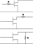
Fig. 2 Low frequency LDMOS device cross-section.

Fig. 3 Simulated I-V characteristics.
When the LDMOS is operating in a multi-tone amplifier, an increase in the number of signals or an increase in the amplitude of the carrier signal could cause the LDMOS device to move into the nonlinear BVcer region (shown by the colored dashed lines), thereby increasing the nonlinearity of the amplifier. This effect could also be exacerbated by increasing the temperature or the operating current of the device. Typical LDMOS circuits attempt to hold the operating current constant by applying a constant gate voltage to the device. A shift in the operating drain current (at a constant gate voltage) can be seen to affect the operating characteristics of the device (hence its linearity) as it gets closer to the nonlinear region.
In very high frequency devices, a second effect comes into play to further complicate both device linearity and reliability. The original device has a relatively deep drain diffusion, which keeps the field in the drain adjacent to the P-channel diffusion relatively small. However, the deep drain diffusion causes the N- to diffuse sideways under the poly gate. This deep diffusion causes the Miller effect capacitance (shown in blue) to increase, which is deadly at high frequencies, since it acts as a negative feedback, reducing gain and circuit stability. For this reason, LDMOS designers are forced into very shallow drain diffusions to minimize the Miller capacitance. Unfortunately, this effect creates a new problem. Now, the applied drain voltage must be depleted across a very narrow region (0.5 µm or less). The increased field in the drain can cause the electrons to have sufficient velocity to actually penetrate into the gate oxide. These are called "hot electrons." They can damage the gate oxide and cause trapped charge in the gate to influence the threshold of the LDMOS device. The threshold change can cause the idling current of the circuit to change, affecting the gain, linearity and stability of the circuit. Both the high drain field, due to the shallow drain diffusion, and the parasitic NPN bipolar affect the hot electron effect, shown by the blue arrows in Figure 4 . The concern about stabilizing the LDMOS device against threshold drift is now complicated by the long-term effects of permanent damage to the gate oxide. This effect is known as time dependant dielectric breakdown (TDDB). Its effects have been well studied for low voltage, thin oxide microcircuits, although its effect for a high voltage, high power device is not known at this time. This certainly complicates the long-term reliability questions about LDMOS devices.

Fig. 4 LDMOS device showing the (a) the parasitic NPN bipolar and (b) the electrons effect.
Currently, manufacturers either perform a short burn-in on their LDMOS devices or attempt to guarantee device lifetime by a sample lot burn-in. If, however, the device is inherently prone to hot electron effects, this screening can only be partially effective. No amount of screening can effectively eliminate TDDB failures from the product mix.
There may be a more effective method of determining the reliability of LDMOS devices than burning them in to screen out threshold drift. As long as a significant hot electron problem exists, screening can catch only a percentage of potential future failures. A good test might well be to simulate both the avalanche condition created by the poor bipolar layout and the hot electron effect by screening the device with a relatively high current in the avalanche breakdown mode, as shown in Figure 5 . The exact level of current the device will encounter that is necessary to insure that both fragile SOA and the hot electron effect are excluded from circuit applications is not known. It should be determined what current would be sufficient to stress the device in the breakdown mode to screen out these devices. If an LDMOS device could pass a reverse breakdown test at 10 percent of maximum rated power in the reverse avalanche mode without device degradation or threshold voltage shift, its reliability in most circuit applications should be improved. A production screen test at full rated power would almost certainly insure its linearity and reliability under any circuit conditions. A device capable of passing this sort of breakdown test is probably not now available. The Shadow LDMOS proposed below should be capable of passing a much more brutal BVdss test than other LDMOS devices, as early devices have shown.

Fig. 5 Typical LDMOS breakdown characteristics.
The Shadow LDMOS
In the early 1980s a non-self-aligned shadow MOSFET technology was developed. By 1984, this technology had evolved to the point where an LDMOS device could be designed using the same technology. The first LDMOS device was developed under a defense program to provide an extremely broadband device capable of 50 W pulsed across the 960 to 1215 MHz radar band. The device proved capable to meet the contract requirements and provided approximately 7 to 8 dB gain across the 255 MHz band. A cross-section of this device is shown in Figure 6 .

Fig. 6 Self-aligned shadow LDMOS device cross-section.
This early device suffered from two serious drawbacks. First, it had a relatively long channel length (0.5 µm), which was acceptable for 1 GHz operation, but limited the device at higher frequencies. The second drawback was the inability to reduce the Miller capacitance. At that time, a thick oxide "bump" could only be aligned to within a half micron, so the Miller capacitance was much higher than the newer device. Nonetheless, this device proved to be an excellent high frequency transistor and it had none of the reliability and operational drawbacks of threshold instability or latch-back that are common today. The device was actually capable of sustaining a reverse breakdown current to an extent that exceeded its maximum power rating. At that time, latch-back was well understood and the shadow isolation process virtually eliminated this as a concern. The hot electron threshold drift was never observed. The lack of a technology to reduce the Miller capacitance did, however, present some small operational concerns, because it did affect the stability of the circuit. Since latch-back was not a concern but circuit stability was, some additional Miller capacitance effects were observed by noting that the gate voltage actually modulated the breakdown voltage of the device. A curve tracer photograph giving an example of this effect is shown in Figure 7 .
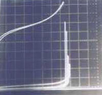
Fig. 7 Gate-modulated breakdown voltage characteristics.
Since then, a new, self-aligned technique was developed to allow a thick oxide bump to be self-aligned over the exposed drain region. This allowed 1.5 µm of oxide under the overlapping gate metal, instead of only approximately 0.1 µm. At the same time, work was nearly completed to allow a reduction of the channel length from 0.5 µm to approximately 0.25 µm. These improvements should allow operation of the new device into the 4.0 GHz range without any hot electron effect and with improved safe operating area and linearity.
A comparison of the self-aligned, shadow isolated LDMOS and the original poly gate LDMOS is shown in Figure 8 . Note that the thicker P- and N- epitaxial layers reduce both the output capacitance and the electric field in the drain region. The effect of the significantly reduced resistance across the parasitic bipolar and the reduced field in the drain should make the self-aligned shadow LDMOS device capable of passing a much more brutal BVdss test, increasing the long-term reliability and improving the device linearity. The shorter channel and reduced output capacitance should also improve its frequency performance. Note that the metal gate will improve the operating symmetry of the device. The early shadow isolated vertical DMOS proved extremely reliable. A cross-section of this device is shown in Figure 9 .
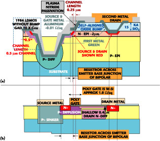
Fig. 8 Comparison between (a) the self-aligned shadow isolated LDMOS and (b) the original poly gate device.
Early on, some production problems developed and tales of threshold instability, cracked gate oxide and zero yield followed. In retrospect, one can surmise that a simple error introduced in the fabrication process led to the problems. The final aluminum metal was actually deposited underneath the overhanging gate oxide and provided the emitter-base short mentioned earlier (note that the source and gate metal were self isolating across the - shadow casting - oxide overhang). The problem arose when the metal was masked to etch away the unwanted metal in the field, and to define the bonding pads. The tiny notches under the gate metal provided an area where the negative photoresist was trapped prior to etching the aluminum. The stripper used to remove the photoresist was unable to get under the overhang to remove the trapped photoresist. This was impossible to see because the aluminum on top blocked the vision of anyone looking down at the device. The solution to this problem is relatively simple. By increasing the temperature of the organic stripper from 90°-100° to 115°-120°C, the resist residue underneath the overhang could be completely removed. However, the stripper degraded over a short period, becoming viscous and after a day or two became unusable. This may have caused abandoning the use of the shadow FET because of increased processing costs.

Fig. 9 Shadow isolated vertical DMOS; (a) before metallization and (b) after metallization.
Conclusion
The LDMOS is a device that can be used in cellular base station transmitters with frequencies up to 4 GHz and powers up to 150 W. Early problems of linearity and reliability have been solved by using a new design called a self-aligned shadow isolated LDMOS. This device was abandoned because of a problem in the fabrication process but could be revived with new technology.
J. Rice has a BS in physics from the University of California at Berkeley and a master's degree in physics from UCLA. He has worked in the semiconductor industry for 30 years and introduced several innovative design concepts into production, primarily high frequency, high power discrete silicon transistors. He holds six process and design related patents including several for alignment techniques, shadow isolated MOSFETs and internal matching for discrete RF transistors. He can be contacted via e-mail at jedrice@yahoo.com.