
Cover Feature
Low Cost Millimeter-wave Packaged MMICs
United Monolithic Semiconductors S.A.S.
Orsay Cedex, France
To this end, this article addresses the issue of reducing the cost of millimeter-wave surface-mount devices (SMD) packaging, and using this technology to produce a full SMD-packaged MMIC chipset for 26 GHz point-to-point and point-to-multipoint radio links. First, reducing costs means increasing the standardization at system, module assembly and component levels, with generic module architectures being developed, perhaps using software defined radio concepts for customization. This will facilitate the development of plug-and-play standard sub-functions and components. In this way generic MMICs with a higher integration level (a full receiver or transmitter macro-function chip, for example) could be designed.
|
Table 1 | |
|
MMICs |
30-35% |
|
Other materials |
5% |
|
Module housing |
15% |
|
Assembly |
20% |
|
Testing and tuning |
25-30% |
Here, the minimization of the MMIC assembly costs by using the SMD packages now available for millimeter-wave applications are considered. By employing SMD packaging future manufacturing of millimeter-wave modules can use standard SMD assembly lines, avoiding the need for expensive pick-and-place, die attachment and wire bonding tools in clean room environments. Of course, before the final module assembly, the bare MMICs must be mounted in packages, and this still requires expensive microelectronic tools. However, MMIC packaging will be limited to specialized units, able to economically realize the high costs of these tools thanks to sufficiently high volumes and standardization.
What needs to be considered is that millimeter-wave SMD packages must be designed in a specific manner to provide low loss RF interconnections, good RF grounding, high thermal conductivity and an easy assembly process. The packaging concept applied by UMS has been developed by HEI and is suitable for frequencies from DC to more than 45 GHz. Due to the flat back face of the chip carriers, the packaged MMICs are real surface-mount devices and, thus, require only a flat printed circuit board (PCB) without any cutouts or special modifications. The previously described chip carrier1 is manufactured using the same soft organic dielectric material as for the chip carrier plate, the walls and lid of the package. The chip carrier base plate is specifically designed for one MMIC (or a family of MMICs with a similar size and pad arrangement) to minimize the length of the bonding wires inside the package. The ground, DC and RF connections are achieved using filled mini-vias across the chip carrier. A large number of small vias are used for ground connections to give a very low inductance and also to minimize the thermal resistance of the package.
A schematic cross-section of a packaged MMIC mounted on an evaluation board is shown in Figure 1 . The packages are designed for optimum performance when mounted on a PCB comprising a soft organic material with a dielectric factor of approximately four and a thickness of 200 µm. Below the package ground pad it is recommended to use a PCB with a large number of small, filled vias to provide a good ground connection, which is essential for optimum RF performance and efficient heat sinking.
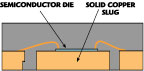
Fig. 1 Schematic of an SMD-packaged MMIC mounted on a printed circuit evaluation board.
An additional advantage of this new package design is related to the self-alignment of the device during the soldering reflow process. Several tests have shown that due to the specific footprint of this package in conjunction with the adhesion of the liquid solder during reflow, the package is forced into the right position by capillarity. This feature reduces the requirement for positioning accuracy, and thus enables handlers with limited precision performance to be used.
Because good blocking of RF at the DC connections is always necessary to prevent MMIC oscillations, first stage DC blocking capacitors in the range of 120 pF are integrated into the package, together with the MMIC chip. This leads to rather insensitive SMDs with respect to feedback loops through DC lines and excellent stability down to the low frequency range. In addition, it relaxes the standard practice of putting RF blocking capacitors close to the packages where handling is always difficult due to limited space. Using this approach a full chipset of Ka-band SMD-packaged MMICs has been developed.
|
Table 2 | ||
|
Part Number |
Function |
Bandwidth (GHz) |
|
CHA2066 |
self-biased LNA, two stages |
10 to 16 |
|
CHA2069 |
self-biased LNA, three stages |
18 to 31 |
|
CHA2093 |
LNA, two stages |
20 to 30 |
|
CHX2090 |
frequency multiplier (2x) |
22 to 26 |
|
CHT3091 |
attenuator |
DC to 40 |
|
CHA2098 |
driver amplifier, 15 dBm |
20 to 40 |
|
CHA3092 |
driver amplifier, 20 dBm |
20 to 33 |
|
CHA5390 |
driver amplifier, 25 dBm |
24 to 32 |
|
CHM1290 |
Rx/Tx converter |
20 to 30 |
|
CHA5093 |
HPA, 30 dBm |
22 to 26 |
The full availability of all MMICs used in a specific front-end architecture is required to ensure the success of this new approach of using SMD-packaged MMICs for microwave and millimeter-wave applications. Just missing one package component in the Tx/Rx chain will result in a return to the cost intensive chip-and-wire technique and prevent significant cost savings. Therefore, a complete chipset has been developed for telecom front-ends at 26 GHz in SMD packages (see Table 2 ). A typical block diagram of this transceiver module is shown in Figure 2 . Both low power MMICs, like multipliers, mixers, and low noise amplifiers (LNA) and high power MMICs, in particular drivers and high power amplifiers where thermal dissipation needs to be optimized, make use of this packaging technology.
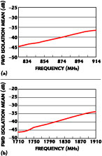
Fig. 2 Block diagram of a 26 GHz transceiver module comprised entirely of SMD-packaged MMICs.
The chipset comprises three different LNAs which can be used either as a first amplifier in the receive path or as a pre-amplifier for the multiplier. Two of these contain a self-biasing network, which minimizes the need for supplying correct voltages to the different amplifier stages. Figure 3 shows the typical gain performance and noise figure for the CHA2066-RBF device. The component exhibits a noise figure in the range of 2 dB, which is fully comparable to the bare die version.
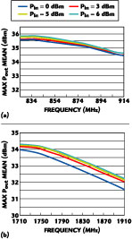
Fig. 3 Measured gain and noise figure performance of three SMD-packaged CHA2066 Ku-band LNAs at Vd =3.5 V and Id =55 mA.
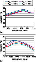
Fig. 4 RF performance of the CHA2069 MMIC measured in a test jig with the MMIC chip mounted directly on the test board and in an SMD package.
The RF performance of the CHA2069 IC, mounted in an SMD package, is shown in Figure 4 , along with a direct comparison to the performance of the die version. It can be seen that the in-band gain variation is slightly higher for the packaged version, which is mainly due to the larger dimensions of the RF transition from the chip to the motherboard leading automatically to higher parasitics. An improvement can be obtained by minor adjustments of the transition structure. Other specifications, in particular the noise figure (see Figure 5 ), are not influenced by this effect and thus remain at the bare die level.
Figure 6 displays the performance of the frequency multiplier for eight different devices. There is a very low variation from device to device and an output power well above 12 dBm. Also, the rejection of the fundamental frequency in the defined frequency band (22 to 26 GHz) always exceeds 15 dBc. The CHM1290 is selected for mixing purposes. Due to the use of diodes and the lack of amplifiers in the RF and IF path, the device can be used both in up-converter and down-converter modes.
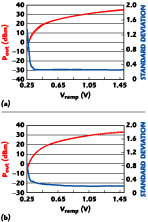
Fig. 5 Measured gain and noise figure performance of an SMD-packaged CHA2069 Ka-band LNA at Vd =4.5 V.
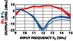
Fig. 6 Measured performance of eight SMD-packaged CHX2090 frequency multiplier MMICs with Pin =12 dBm.
As already mentioned, the success of MMICs in SMD packages on the worldwide market is directly linked to the availability of a full chipset in SMD-type packages. In this respect high power amplifiers are the most critical components, due to their high thermal dissipation. Taking this approach for a full 26 GHz MMIC chipset, four different drivers and high power amplifiers have been realized. For the corresponding measurement the components were mounted on a test board containing a sufficiently large heat sink. Figure 7 shows the gain compression curves of the CHA5390 exhibiting a very broadband (24 to 30 GHz) performance with an output power level of well above 24 dBm.
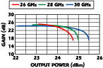
Fig. 7 Gain compression vs. frequency curves of an SMD-packaged CHA5390 Ka-band driver amplifier at Vd =5 V and Ids =460 mA.
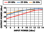
Fig. 8 Measured power performance of an SMD-packaged CHA5093 HPA MMIC at Vd =6 V and Ids =600 mA.
Finally, the CHA5093 high power amplifier (HPA) demonstrates the capabilities of this packaging technology to deal with RF power levels in excess of 1 W (see Figure 8 ). The P1dB compression point at approximately 29 dBm is achieved with a corresponding gain in the range of 20 dB. The DC power consumption with no RF input power applied is (6V, 600mA) 3.6 W. A currently running reliability test has shown no degradation after 2,000 hours, indicating the capability of this specific packaging concept to deal with RF power levels in the range of 1W.
SMD MMIC packaging offers a breakthrough for significantly lowering the cost of millimeter-wave front-end modules. In the future these modules will be manufactured using standard SMD assembly lines, avoiding high cost microelectronic tools in clean room environments. Figure 9 shows a 26 GHz transceiver working prototype manufactured by Thales Microwave, using only SMD-packaged MMICs and assembled on an industrial SMD line. This module comprises SMD-packaged MMICs originating from various MMIC sources (Alpha Industries, Hittite, UMS), demonstrating that such a solution does not require one single MMIC supplier and that some standardization already exists.
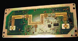
Fig. 9 A working transceiver module for 26 GHz point-to-point radio link applications.
Conclusion
A full SMD-packaged 26 GHz MMIC chipset has been demonstrated for point-to-point or point-to-multipoint radio link applications. This chipset includes LNAs, driver amplifiers, a frequency multiplier, an attenuator, a sub-harmonic mixer and finally a 1 W HPA, demonstrating that this packaging concept is also applicable for power devices. All of the packaged circuits exhibit excellent performance, identical or close to those of unpackaged devices and are now available for volume production. Additional information may be obtained via e-mail at klaus. beilenhoff@ums-gaas.com.
References
1. "A DC to 50 GHz and Beyond MMIC Carrier," Microwave Journal , Vol. 44, No. 9, September 2001, p. 236.
United Monolithic Semiconductors S.A.S., Orsay Cedex, France.
Circle No. 301