
Technical Feature
A Distributed Amplifier for 40 Gbps Fiber-optic Communications Systems
H. Shigematsu, M. Sato, T. Hirose and Y. Watanabe
Fujitsu Laboratories Ltd.
Atsugi, Japan
In recent years, the rapid development of multimedia communications has generated a strong demand for high speed and high capacity transmission systems. Wavelength-division multiplexing (WDM) and time-division multiplexing (TDM) have been developed to realize the next generation of transmission systems. Ultra-high capacity transmission experiments have been reported1,2 using a WDM system with data-rate performances of 40 Gbps per channel. A 40 Gbps transmission system makes animated-data communications feasible. High speed integrated circuit (IC) technologies with data rates of 40 Gbps are required for both WDM and TDM systems. ICs with various devices have been developed for practical use.3-11
Fig. 1 Block diagram of a 40 Gbps fiber-optic transmission system.
Figure 1 shows a block diagram of a 40 Gbps fiber-optic transmission system. A LiNbO3 modulator driver and a preamplifier are key components of the system. The LiNbO3 modulator driver, which is located at the front-end of the transmitter, plays a role in amplifying the signal from the multiplexer to the more than 5 Vp-p output needed to drive a LiNbO3 modulator. The preamplifier, whose input is connected to a PIN photodiode, is located at the front-end of the receiver's optic to electric conversion. It amplifies a very small photo current to a voltage large enough to drive the next ICs. Although the input 40 Gbps data has various frequency components, a bandwidth greater than 40 GHz and a flat gain are required to amplify this waveform accurately. High speed IC technology for over 40 Gbps (for example, 80 Gbps) will also be required in the future. In particular, what kind of circuit structure is needed to meet this high speed requirement must be considered. Figure 2 shows schematics of a conventional lumped amplifier and a distributed amplifier. In a cascaded configuration, the total gain of a conventional lumped amplifier is one if the gains of the individual transistors are close to one as the frequency increases. Therefore, a conventional lumped amplifier cannot amplify an input signal at very high frequencies. The total gain of a distributed amplifier is given by the sum of each stage, nG/2, not their product. The total gain of a distributed amplifier becomes n/2, when the gains of the transistors are close to one. This means that a distributed amplifier has a wider bandwidth than a lumped amplifier.
Fig. 2 Schematics of a (a) lumped and (b) distributed amplifiers.
Figure 3 shows the gain vs. frequency of a lumped and a distributed amplifier. The gain potential of the transistors is utilized in a distributed amplifier design because its matching circuits are made of loss-less reactive (LC) components. The cut-off frequency of a lumped amplifier is much lower than that defined by the maximum available gain of a transistor, because resistors, which are lossy elements, are used in the matching circuits. Furthermore, the amplifier consists of transistors connected in parallel resulting in large currents and producing a large output power. Therefore, a distributed amplifier is chosen for the modulator driver circuit.
While a distributed amplifier is promising for use in this application, its electrical parameters must be finely optimized to meet the stringent requirements, including high output power, high gain, flat gain and broad bandwidth. Simply using several stages to obtain high output power increases the gain ripple and degrades stability. In this article, a distributed amplifier designed with stabilization, negative resistance control and broadband impedance matching for a 40 Gbps LiNbO3 modulator driver circuit is described. The design makes it possible to achieve a 54 GHz bandwidth and a 6 Vp-p output at 40 Gbps. An InP-based preamplifier, to which this design was applied, is also discussed.
Fig. 3 Gain vs. frequency for a lumped and distributed amplifier.
Circuit Design
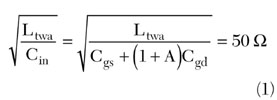
First, the basic design of a conventional distributed amplifier is outlined, as illustrated in Figure 4 . The procedure for designing a distributed amplifier is to first add an inductance Ltwa to an input transmission line to satisfy the following equation in a 50 ohms system
where
A = gain of a transistor
Co is continuously added to the output transmission line to satisfy the equation of Cin = Cds + Co .
Co consists of distributed transmission lines. Moreover, Ltwa is also added to the output transmission line. This allows the condition of phase velocity and characteristic impedance to be satisfied. The cut-off frequency is defined approximately by
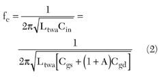
Here, a transistor with a small input capacitance is required. If a transistor with a large input capacitance is used, a large Ltwa is required to satisfy the characteristic impedance condition. However, this degrades the cut-off frequency because the product of Ltwa and Cin is large. Therefore, a transistor with small Cgs should be used in an ultra-broadband amplifier.
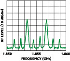
Fig. 4 Schematicof a conventional distributed amplifier.
To obtain a wider bandwidth, a cascode configuration is suitable. In a cascode configuration, the Miller capacitance, (1 + A) Cgd , can be neglected and Cin = Cgs . Therefore, an ultra-broad bandwidth can be achieved. However, there are two problems with using a conventional distributed amplifier in a fiber-optic communications system. The first is a forward gain slope; the other is a gain ripple at high frequencies. The gain slope, which is caused by losses in the input and output transmission lines, must be compensated for. Gain ripples are caused by the return loss degradation at high frequencies. To suppress them, it is important to achieve good impedance matching within the whole bandwidth.
The techniques to solve these problems will be explained in detail. To solve the first problem, namely, to compensate the gain slope, the design of the unit cell is quite important. Figure 5 shows the equivalent circuit of a cascode pair of transistors. In a conventional cascode configuration, the output impedance of Ql seen from the source terminal of Q2 without a source inductance Ls is always capacitive because of the drain-source capacitance (Cds1 ) of Q1. Therefore, a positive feedback circuit is formed. This configuration generates a negative resistance, thus compensating for the loss of the transmission lines. However, a drastic increase in negative resistance also degrades the stability of the amplifier when it is operating at around the cut-off frequency. To suppress the negative resistance, a source inductance Ls is inserted between the source of Q1 and ground, and a circuit consisting of Lcg , Rgate and Cgate is connected to the gate of Q2. There is an option to change the gain profile of the circuit so that it produces a flat amplifier gain profile.12
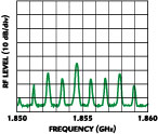
Fig. 5 Equivalent circuit of a cascode pair of transistors.
Figure 6 shows the gain vs. frequency with and without Ls . Ls maintains the gain flatness and improves the stability and bandwidth. In this simulation, Ls is 20 pH and the other parameters are fixed. The K-factor of the amplifier without Ls was below 1.0 in portions of the bandwidth and the circuit was unstable. The K-factor was increased above 1.4 by inserting Ls .
Fig. 6 Simulated gain and K-factor vs. frequency with and without Ls .
The gain ripple can be suppressed as follows. Figure 7 shows a schematic of a distributed amplifier with an input matching circuit. The return loss of a conventional distributed amplifier degrades as the frequency increases. An impedance matching circuit was designed to increase the input-return loss around 40 GHz by using a pad capacitance, the source inductance of Q1, and a line between the input port and the first stage. In the conventional design of a broadband amplifier, a narrow band impedance matching is not performed. However, a broadband impedance matching between near DC and approximately 50 GHz was attempted by the above method. Figure 8 shows the calculated gain response with and without an impedance matching circuit. The input-return loss with an input matching circuit is greater than that of an amplifier without an input matching circuit between 35 and 45 GHz. The gain ripples at high frequencies were also suppressed. A low frequency extension circuit is also briefly explained. The output termination circuit consists of an on-chip capacitance and a large off-chip capacitance. The chip includes a damping resistance to remove the resonance caused by the wire. This structure has the advantage of being easy to assemble.
Fig. 7 Distributed amplifier with input matching circuit.
Grounded coplanar waveguide (GCPW) lines with a 75 mm thick substrate were used in the circuit design to make the chip easy to mount and to perform on-wafer DC and RF measurements. A conventional microstrip line (MSL) chip needs via holes for normal operation. Therefore, a MSL chip cannot be used for on-wafer measurements. A CPW structure leads to a chip cost lower than for a MSL structure. The S-parameters of 600 mm thick coplanar waveguide (CPW) lines and 75 mm thick GCPW lines, 1 mm long, were calculated. The line width and the gap were both 20 mm. The CPW and GCPW structures have similar characteristics. The characteristic impedance of a 600 mm CPW is 52 W and that of a 75 mm GCPW is 50 W. The losses of both lines were 0.3 dB/mm. The simulated gain response of a distributed amplifier with GCPW lines is the same as one with CPW lines. To obtain an output voltage swing of over 5 Vp-p, the distributed amplifier consists of eight stages with cascode-configured unit cells. The gate width of each transistor is 80 mm.
Fig. 8 Calculated S-parameters with and without matching circuit.
Fabrication
The distributed amplifiers were fabricated using double-doped AlGaAs/InGaAs/AlGaAs pseudomorphic HEMTs (pHEMT). The gate was a T-shaped structure made of aluminum. The gate length of 0.15 mm was formed by using electron beam lithography. The source and drain electrodes were made of AuGe/Ni/Au. The device consisted of a channel layer sandwiched between two electron supply layers. The transconductance gm and the maximum drain current Idsmax were 525 mS/mm and 560 mA/mm, respectively. The cut-off frequency at Vgs = -0.1 V and Vds = 3.0 V was 90 GHz. The resistors were made from epitaxial layers that had a sheet resistance of 120 W per square. The MIM capacitors were made from SiN.
Figure 9 shows a microphotograph of the distributed amplifier. GCPW lines with via holes were used. Ground via holes were placed at the source terminals to achieve an accurate Ls as required by the design. This structure is suitable for a face-up assembly and enables RF performance to be checked without having to use the via holes. Ground-bridge interconnects were also used to avoid undesired modes. It is important to make the grounds of the circuit stable when designing high frequency circuits. The grounds cannot fulfill their function if there are small inductive components at high frequencies. The GCPW structure also suppresses the coupling of adjacent lines. The chip was 4.2 x 1.6 mm and its power consumption was 1.1 W.
Fig. 9 The distributed amplifier 4.2 x 1.6 mm chip for the LiNbO3 modulator driver.
Circuit Performance
The S-parameters were measured using an HP8510XF vector network analyzer. RF probes were calibrated using the LRRM method.
Figure 10 shows the frequency characteristics of the 75 mm GCPW chip. Very good performance was achieved with a 15 dB gain and a 54 GHz bandwidth at a drain bias of 6 V and a gate bias of -0.1 V. This is the highest gain bandwidth product ever reported for baseband amplifiers fabricated using GaAs-based FETs, which can be applied to an optical transmission system. These results indicate that this circuit design is suitable for extending the bandwidth of an amplifier and making it stable. The gain ripple was within ±0.5 dB. The deviations in group delay were approximately ±10 ps up to 40 GHz. The input- and output-return losses were greater than 15 dB and 10 dB up to 50 GHz, respectively. The input impedance matching circuit provided a low input-return loss up to 50 GHz as expected. In comparison, the bandwidth of the 600 mm thick substrate was 45 GHz. The reason the bandwidth was wider than for the 600 mm thick substrate was the stable source ground vias. The source inductance for a 600 mm substrate is larger than that of a chip with via holes. The source ground of a CPW distributed amplifier is very important to achieve a wide bandwidth using flip-chip bonding or via holes.
Fig. 10 Frequency response of the distributed amplifier.
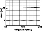
Fig. 11 Low frequency gain characteristics of the distributed amplifier.
Figure 11 shows the low frequency characteristics between 100 kHz and 200 MHz of a distributed amplifier connected by a 2.2 nF and 1.0 mF capacitor to the EXT terminal. The gain profile was quite flat and no ripple and peaking were observed. A -2 dB low frequency cut-off at 50 kHz was also observed.
Figure 12 shows the Pout vs. Pin characteristics for a drain bias of 6.0 V at 20 GHz, which is a fundamental frequency for 40 Gbps data. A P1dB of 20 dBm was obtained, which corresponds to 6.3 Vp-p in a 50 W load. The saturated power (Psat ) was 23 dBm. A Psat of 20 dBm was also obtained at 40 GHz. Figure 13 shows an eye-diagram of the output at 40 Gbps. A linear and clear 6 Vp-p output voltage swing was observed. These results indicate that this circuit is promising for a LiNbO3 modulator driver. A module can be fabricated with a 30 dB gain using only two chips. A two-chip configuration reduces the power consumption of the module.
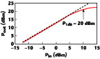
Fig. 12 Output power vs. input power at 20 GHz.
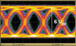
Fig. 13 Output waveform of the LiNbO3 modulator driver.
The above design techniques were applied to an InP HEMT IC. Figure 14 shows the frequency characteristics of the distributed amplifier. A gain of 12 dB and a bandwidth of 76 GHz were obtained. The transconductance of an InP HEMT is greater than that of a GaAs HEMT. Consequently, smaller-size transistors can be used in a distributed amplifier design to achieve a wider bandwidth.
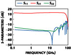
Fig. 14 Frequency characteristics for an ImP HEMT-based distributed amplifier.
Figure 15 shows a chip photograph of the preamplifier, in which the distributed amplifier described above is used. The chip size is 3.1 x 1.8 mm. HEMTs with a gate width of 40 mm were used in the distributed amplifier. Coplanar waveguide lines with ground-bridge interconnects were also used to avoid undesired modes. The width of the coplanar waveguide lines is 20 mm. The characteristic impedance is 68 W. The power consumption of the IC is 0.52 W.
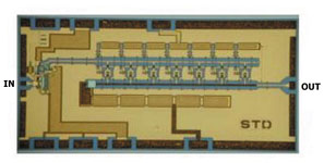
Fig. 15 Chip photograph of the preamplifier.
Figure 16 shows the frequency characteristics of the preamplifier. A transimpedance gain of 52 dBW and a bandwidth of 49 GHz were achieved. To the author's knowledge, this is the highest transimpedance gain-bandwidth product of any reported, over 40 GHz, preamplifiers. The gain flatness of this preamplifier is also better than that of any preamplifier yet reported. The gain (S21 ) was 20.4 dB. The input impedance was 31 W, and the output-return loss (S22 ) was greater than 10 dB up to 50 GHz. A low input impedance plays an important role in widening the total bandwidth of a preamplifier connected to a PIN photodiode. These results also indicate that the circuit design is suitable not only for 40 Gbps preamplifiers but also for other wide bandwidth amplifiers.
A module, consisting of a preamplifier connected with a PIN photodiode, was fabricated. Figure 17 shows the output waveform of the PIN preamplifier module at 40 Gbps. A clear eye-pattern was obtained.
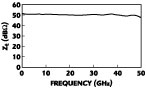
Fig. 16 Transimpedance gain vs. frequency for the preamplifier.
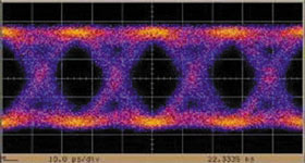
Fig. 17 Output waveform of the preamplifier.
Conclusion
A distributed amplifier for a LiNbO3 modulator driver is described which uses double-doped AlGaAs/ InGaAs/AlGaAs pseudomorphic HEMTs. A 15 dB gain and a 54 GHz bandwidth were obtained with GCPW lines, as well as a 6 Vp-p output at 40 Gbps. These results indicate that the distributed amplifier is an excellent candidate for the LiNbO3 modulator-driver circuit in 40 Gbps fiber-optic communication systems. A preamplifier was also developed with a 52 dBW transimpedance gain and a 49 GHz bandwidth, using an InP-based distributed amplifier. A clear output waveform for a module consisting of the preamplifier connected to a photodiode at 40 Gbps was observed.
Acknowledgments
The authors wish to thank Mr. K. Makiyama, Mr. H. Hirano and Mr. Tateno for the device processing, and Dr. M. Takigawa and Mr. H. Ohnishi for their encouragement and support.
References
1. Y. Yano, T. Ono, K. Fukuchi, T. Ito, H. Yamazaki, M. Yamaguchi and K. Emura, "2.6 Terabit/s WDM Transmission Experiment Using Optical Duobinary Coding," ECOC'96 Postdeadline Papers , ThB. 3.1, 1996.
2. S. Kuwano, N. Takachio, K. Iwashita, T. Otsuji, Y. Imai, T. Enoki, K. Yoshino and K. Wakita, "160 Gbit/s (4 ch ´ 40 Gbit/s electrically multiplexed data) WDM Transmission Over 320 km Dispersion-shifted Fiber," OFC'96 Postdeadline Papers , PD25, 1996.
3. M. Wurzer, J. Bock, H. Knapp, W. Zirwas, F. Schumann and A. Felder, "A 40 Gbps Integrated Clock and Data Recovery Circuit in 50 GHz fT Silicon Bipolar Technology," IEEE Journal of Solid-state Circuits , Vol. 34, No. 9, September 1999, p. 1320.
4. T. Otsuji, Y. Imai, E. Sano, S. Kimura, S. Yamaguchi, M. Yoneyama, T. Enoki and Y. Umeda, "40 Gbps ICs for Future Lightwave Communications Systems," IEEE Journal of Solid-state Circuits , Vol. 32, No. 9, September 1997, p. 1363.
5. J. Godin, M. Riet, S. Blayac, Ph. Berdaguer, J.L. Benchimol, A. Konczykowska, A. Kasbari, P. Andre and N. Kauffmann, "Improved InGaAs/InP DHBT Technology for 40 Gbit/s Optical Communication Circuits," IEEE GaAs IC Symposium , 2000, pp. 77-80.
6. T. Masuda, K. Ohhata, F. Arakawa, N. Shiramizu, E. Ohue, K. Oda, R. Hayami, M. Tanabe, H. Shimamoto, M. Kondo, T. Harada and K. Washio, "45 GHz Transimpedance, 32 dB Limiting Amplifier and 40 Gbps, 1:4 High Sensitivity Demultiplexer with Decision Circuit Using SiGe HBTs for 40 Gbps Optical Receiver," International Solid-state Circuits Conference , 2000, p. 60.
7. M. Mokhatari, T. Swahn, R.H. Walden, W.E. Stanchina, M. Kardos, T. Juhola, G. Schuppener, H. Tenhunen and T. Lewin, "InP HBT Chip-set for 40 Gbit/s Fiber Optical Communication Systems Operational at 3 V," IEEE Journal of Solid-state Circuits , Vol. 32, September 1997, pp. 1371-1382.
8. H. Masuda, K. Ouchi, A. Terano, H. Suzuki, K. Watanabe, T. Oka, H. Matsubara and T. Tanoue, "High Performance InP/InGaAs HBTs for 40 Gbps Optical Transmission ICs," IEICE Transactions on Electronics , Vol. E82-C, No. 3, March 1999, pp. 419-427.
9. M. Sokolich, C.H. Fields, S. Thomas, III, B. Shi, Y.K. Boegeman, M. Montes, R. Martinez, A.R. Kramer and M. Madhav, "A Low Power 72.8 GHz Static Frequency Divider in AlInAs/InGaAs HBT Technology," IEEE Journal of Solid-state Circuits , Vol. 36, September 2001, pp. 1328-1334.
10. T. Suzuki, H. Kano, Y. Nakasya, T. Takahashi, K. Imanishi, H. Ohnishi and Y. Watanabe, "40 Gbit/s D-type Flip-flop and Multiplexer Circuits Using InP HEMT," IEEE International Microwave Symposium Digest , 2001, pp. 595-598.
11. H. Suzuki, K. Watanabe, K. Ishikawa, H. Masuda, K. Ouchi, T. Tanoue and R. Takeyari, "Very High Speed InP/InGaAs HBT IC's for Optical Transmission Systems," IEEE Journal of Solid-state Circuits , Vol. 33, No. 9, September 1998, p. 1313.
12. H. Shigematsu, M. Sato, T. Suzuki, T. Takahashi, K. Imanishi, N. Hara, H. Ohnishi and Y. Watanabe, "49 GHz Preamplifier with a Transimpedance Gain of 52 dBW Using InP HEMTs," IEEE Journal of Solid-state Circuits , Vol. 36, September 2001, pp. 1309-1313.