
Technical Feature
Designing a Bluetooth Transceiver in RF CMOS
Bob Koupal and Marshall Wang
Signia Technologies
Milpitas, CA
Cory Edelman
Agilent Technologies
Westlake Village, CA
The design of a 2.4 GHz Bluetooth transceiver RFIC in CMOS requires careful verification of key performance criteria at all stages of the design process. This can be accomplished by using electronic design automation (EDA) software that provides for the use of integrated foundry models, system compliance test templates which incorporate Bluetooth test signals and links to test instruments for verification in order to predict measured results from simulation data.
Bluetooth Design Issues
Short-range wireless transceivers using the Bluetooth standard are expected to become embedded in a wide range of devices, including notebook computers, printers, fax machines, cameras, cell phones, headsets, home appliances, PDAs and other portable computing devices. To meet the requirements of size, power consumption and low cost, a system-on-chip (SoC) solution using a high level of integration is required. The goal is to eliminate expensive external components such as surface acoustic wave (SAW) filters and inductors, which minimizes the number of external passive components and eliminates the need for external RF tuning elements, thus making the IC simple to implement in high volume applications.
Bluetooth radio links use the unlicensed 2.4 GHz industrial, scientific and medical (ISM) band with a signal that is frequency hopped over eighty 1 MHz channels at a rate of 1600 hops per second. Any Bluetooth design solution must be able to operate reliably in the presence of other RF emitters in the 2.4 GHz band, including other Bluetooth devices, cordless telephones, microwave ovens and wireless LAN systems such as those using the IEEE 802.11 standard.
Although a single-chip radio has been a stated goal for many wireless standards such as GSM and CDMA phones, Bluetooth is the first standard not only designed to allow high levels of integration, but to demand it in order to achieve the requirements of small size and low cost. Bluetooth IC designs require increasing levels of complexity as radio, mixed signal and digital functional blocks are combined on a single chip of silicon, or even when the overall solution is spread over two separate ICs.
A Two-chip SoC Solution
A two-chip Bluetooth SoC solution is implemented that provides a 2.4 GHz transceiver IC and a baseband controller IC. This approach optimizes the bill of materials (BOM) costs and provides the greatest flexibility in the number of applications it can address. The radio IC, shown in Figure 1 , contains a cascode-type low noise amplifier (LNA) with a source degenerating inductor for noise matching and a 50 W input impedance. The LNA achieves a 4 dB noise figure, 15 dB gain and a -10 dBm input third-order intercept point (IIP3) at 2.45 GHz. The chip also contains an IF filter, mixer and demodulator on the receive side, plus a mixer, filter and power amplifier (PA) on the transmit side. The PA is matched to 50 W using an on-chip high Q inductor and delivers 20 dB gain, +8 dBm P1dB and a power-added-efficiency of 15 percent at P1dB.

Fig.1 Signia Ulysses SBT 5010 Bluetooth transceiver block diagram.
The chip also contains a Gaussian frequency-shift keying (GFSK) modulator/demodulator, a 2.4 GHz phase-locked loop (PLL), a quadrature voltage-controlled oscillator (VCO), tunable IF filters, a digital clock recovery circuitry and DC estimation and control logic. The VCO is a complete RFIC design with an on-chip resonator and frequency tuning varactor circuits. The core VCO consumes only 5 mA for quadrature output at 2.45 GHz. The single-sideband phase noise has a 10 to 15 dB margin to the Bluetooth specification. The primary simulation methods used in the transceiver IC are shown for each of the main functional blocks. The baseband IC contains the entire core Bluetooth functionality, with interfaces for USB, UART and an innovative host interface that allows the controller to be configured for PCMCIA, parallel/printer port and PCI interfaces without the need for additional components. The two chips communicate through an 8-pin BlueRF mode-2 bi-directional interface. This article focuses on the design methods used to implement the RF component of the chipset.
RF Design Methods
Because of its complexity, the design of a Bluetooth radio SoC requires a different approach to simulation and layout. A traditional RF building-block design would begin with component specifications, a circuit topology would be selected and simulation would be performed using harmonic balance or envelope simulation. In SoC design, several disciplines are required simultaneously, since portions of the circuit are high frequency analog, portions are mixed signal (requiring both SPICE-like simulations and Verilog for timing analysis) and the remainder are purely digital (requiring only Verilog simulation). In this design, there are several hundred active components in the analog portion, and over 30,000 gates on the digital side. The complexity of this design prevents the designer from using a single EDA tool for simulating the entire chip, so careful planning must be done at the system level to ensure that each of the individual blocks of the design are specified correctly.
Among the first and most important system parameters are those that define the power and noise budgets. Bluetooth is nominally a 1 mW (0 dBm) system, designed for short-range operation and low interference to other wireless systems. It uses a GFSK modulation in a 1 MHz bandwidth, which together with a 0.1 percent bit error rate (BER) requirement, implies a carrier-to-noise (C/N) ratio of 21 dB. The thermal noise floor for a 1 MHz bandwidth is -114 dBm. The Bluetooth specification demands a receiver sensitivity of -70 dBm or better, which is the power level at a range of ten meters. This specification implies a maximum receiver noise figure of 23 dB. Realistic applications of Bluetooth, however, demand a 10 to 15 dB better receiver sensitivity to overcome fading in the difficult indoor propagation environment where it will most often be used (Figure 2 ).

Fig. 2 Signal and noise levels that define the Bluetooth receiver sensitivity.
Given the requirements for Bluetooth, there are many options for selecting a process technology. BiCMOS, SOI or SiGe may be used, but the lowest cost process available is CMOS. A 0.25 mm CMOS process is typically 30 to 50 percent lower in cost than comparable BiCMOS processes because it requires fewer mask and process steps. Both SOI and SiGe have more expensive starting materials and increased process complexity. CMOS achieves its low cost through high volume, and there are numerous foundries that provide commercially available CMOS capacity. The mature 0.25 mm process used provides an fT of more than 30 GHz and can produce the RF blocks necessary for radio system design - a 3.5 dB noise figure LNA with 20 dB of small signal gain over narrow bands, a fully integrated VCO with quadrature output and phase noise better than -95 dBc/Hz at 500 kHz offset, and a fully integrated 10 dBm PA with 30 percent efficiency. The process is tailored for analog RF design and includes thick top metal allowing the creation of high Q inductors and transformers, metal-insulator-metal (MIM) capacitors, multiple VT devices allowing more flexible analog designs and varactor diodes. The process also has deep-N-well structures that improve device isolation. Using this CMOS process, RFICs with all of the necessary Bluetooth functionality can be created for the lowest possible cost.

Fig. 3 Superheterodyne receiver architecture.

Fig. 4 Zero-IF receiver architecture.
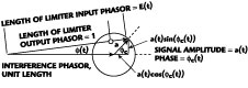
Fig. 5 Low IF receiver architecture.
The next step in the design phase is to select a topology or architecture. Beginning with the receiver, Bluetooth specifications require at least a -70 dBm sensitivity with a BER of 0.1 percent, even with interference present, which is often increased to better than -80 dBm for most applications. For cost and manufacturability, this performance must be achieved with a minimal number of external components. There are three basic receiver architectures that may be considered: the traditional superheterodyne, a low IF and a zero-IF receiver (Figures 3 , 4 and 5 , respectively). Each offers many trade-offs in performance and complexity. Their merits in a Bluetooth application can be summarized. The superheterodyne topology easily meets the electrical requirements, has high channel selectivity and is a well understood circuit; however, it requires an external SAW filter making it too expensive for the Bluetooth requirements. The zero-IF design allows high levels of integration and eliminates the need for an image filter, but often imposes DC offsets onto the output signal and offers poor rejection of local oscillator (LO) feed-through, making zero-IF a relatively complex design to implement. The low IF approach selected also supports high levels of integration and eliminates the need for external filters, but is relatively simple to implement compared to the zero-IF approach, leading to higher yields and lower cost.
Once the low IF receiver architecture is selected, the next decision to be made is whether to use limiter-based or inphase-quadrature (I-Q) demodulation. I-Q receivers are commonly used in digital communication circuits for quadrature phase shift keying (QPSK) demodulation, but require the generation of matched quadrature LO signals and a high linearity automatic gain control (AGC) amplifier. The limiter-based method is well suited for 2-FSK applications and is much simpler to implement, eliminating the need for the AGC amplifier which, again, lowers the cost. Another design choice is to match the front-end of the receiver to 50 W in order to eliminate the need for external matching networks. The entire low IF topology was verified in simulation using high level behavioral blocks included in Agilent EEsof's Advanced Design System 2001 Bluetooth Design Guide,1 and optimized to meet the system performance requirements.
For the transmitter selection, the Bluetooth specification permits three levels of output power, with class 3 at a maximum of 0 dBm, class 2 at +4 dBm and class 1 at +20 dBm, enabling a range up to 150 meters. Typically, the +20 dBm application is implemented using an external PA, so most IC implementations are class 2 or 3. Care was taken to keep the 2 MHz spur of the transmitter below -40 dBc to maintain transmitter performance within specifications when an external PA is added. For determining the optimum transmitter topology, two approaches were considered: direct VCO modulation and I-Q modulation. The direct VCO approach is attractive because it is a simpler design and requires less current, but it is prone to problems with frequency drift and variation of the modulation index. The approach selected for this design is I-Q modulation, which effectively eliminates frequency drift problems and allows direct modulation using I and Q signals derived from the baseband IC. As with the receiver, the entire transmit topology was verified using the Bluetooth Design Guide.
Implementing the Designs
Once the topologies were selected, the RF circuits were simulated using the harmonic balance simulation engine in conjunction with RF models provided by the foundry in the form of a design kit. The design kit has symbols created for each supported device type in the library, including corner models. The user selects a symbol from the library, places it in the schematic and enters the physical dimensions of the device. Callback functions are used to verify that the physical dimensions are within the allowed range. The scaled models are then automatically generating during netlisting. The supported devices include a variety of BSIM3 models for NMOS and PMOS transistors, MIM capacitors, a number of polysilicon and diffused resistors, inductors, varactors and other diodes. BSIM3 models provide a standardized physical description of the relevant parameters for each active device type in the chosen RFIC foundry process. The parameters are typically derived or extracted from measurements performed by an automated modeling system.
For specific inductor values or for the design of on-chip baluns that are not supported by the design kit, the devices are first laid out using Cadence Analog Artist, and then imported into ADS's Momentum 2.5D electromagnetic simulator. Pins are added to the layout to define the current flow direction, the polygons are meshed into rectangles and triangles, and the dielectric properties of the substrate are defined. The circuit is then simulated using the planar field solver, and resulting S-parameters are created and stored in a model file. This file can then be attached to a symbol for use in circuit simulation.
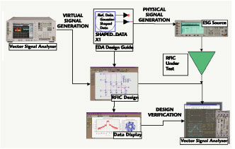
Fig. 6 Bluetooth signal source (ESG) and vector signal analyzer operated by the EDA design guide to verify the RFIC.
At some point, samples will be received from the first tape-out and must be tested. Often, the only measurements available this early in the process are based upon simple sinusoidal sources, which allow only basic verification steps to be performed, such as gain, output power and other measurements focused primarily in the frequency domain. While this will show that the RFIC is somewhat functional, it does not provide confidence that it will work in its intended application. Hence, it is desirable for application-specific test set-ups to be available. There are a number of dedicated signal sources available that feature a Bluetooth personality, along with complementary signal analyzers. However, unless this equipment can be linked into the simulation environment, one cannot be assured that the same stimuli and measurement algorithms that were used in the initial design phase will also be available in the lab. Such test instruments allow the designer to connect to the EDA software in a way that ensures that identical, realistic Bluetooth test signals and measurement algorithms are used for simulation and hardware design, as shown in Figure 6 . In addition, it is possible to insert simulation models into the signal path at any point. These models may include portions of the circuit that are not part of the RFIC, or they may be signal impairments such as multi-path fading. Interfering signals of any type, not just Bluetooth, can be introduced and their effects observed. This has been of great concern with increasing use of WLAN systems in the same 2.4 GHz band, as well as the presence of non-communication-related emitters such as microwave ovens. The Bluetooth 1.1 specification spells out what is required for compliance: receiver sensitivity, adjacent channel interference at various frequency offsets, co-channel interference and intermodulation distortion. For each of these tests, the system must achieve a BER of 0.1 percent. This is the so-called "raw" BER that does not include the improved performance gained by error-correcting coding. Figure 7 shows an adjacent channel sensitivity test, which is critical to the low IF receiver filtering abilities.

Fig. 7 Adjacent channel sensitivity test of the low IF receiver.
Once the design is verified in ADS, the RF schematics are transferred to the Cadence Analog Artist environment using Agilent EEsof's Intermediate-File-Format (IFF) for layout and verification. The blocks are then combined with the mixed signal and digital blocks for final assembly and verification.
Verifying the Design Using Compliance Templates
Figure 8 shows a typical test template that is implemented in both an EDA environment and in bench-test equipment used for hardware design and verification. The circuit under test is inserted in place of the reference transmitter and/or receiver that may be compared with the actual simulated design until the hardware becomes available. A simple additive white Gaussian noise (AWGN) or multi-path model optimized for indoor propagation is inserted into the signal path. Performance may be observed by using an eye diagram (Figure 9 ), a BER measurement (Figure 10 ) showing that the receiver comfortably exceeds the -70 dBm requirement of the Bluetooth specification and should be usable to -83 dBm, or via a software-based vector signal analyzer to demodulate the signal and measure modulation accuracy (Figure 11 ).
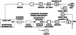
Fig. 8 Receiver sensitivity template.

Fig. 9 Eye diagrams at the receiver demodulation output with input levels of (a) -70 and (b) -84.5 dBm.
For complete and accurate verification, it is essential to have a variety of simulation methods available. Simple checking of a circuit design can be started using nonlinear steady-state techniques such as harmonic balance. Single or multiple tones and their harmonics are found, applicable to system blocks such as mixers, amplifiers and filters. In addition, the use of I-Q modulation with direct up-conversion to the desired transmit frequency in a single step is favored in Bluetooth transceivers. It is difficult, if not impossible, to infer the quality of performance using tone excitation; the full I-Q representation of the modulated signal must be used to drive the modulator if its efficacy is to be determined. Although a transient simulation can infer some aspects of modulator performance, only an envelope simulator can predict it fully. Therefore, the EDA environment must provide either the signal-processing necessary to produce the I-Q representation of the Bluetooth signal and be able to apply the envelopes to the circuit being evaluated, or that signal must be created ahead of time and stored in a format usable by the envelope simulator.

Fig. 10 BER vs. input signal power at the receiver.
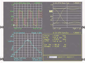
Fig. 11 Vector signal analyzer measurement of the received signal's (a) demodulated symbols,
(b) eye diagram, (c) data statistics and (d) signal spectrum.
In the final phases of the design process, the schematic was transferred to a layout environment and subjected to time-domain simulation as an additional verification step. Following the layout entry and design rule check, a GDSII stream was produced and sent to the foundry. Finally, the fabricated devices were verified in a full transmit or receive configuration, again using the EDA-based test templates and associated test equipment.
Results
The simulations were performed using both steady-state and time-domain methods. Harmonic balance techniques were appropriate for the initial design of the I-Q modulator, power amplifier, LNA and mixer subcircuits. Two time-domain methods were used: SPICE and Envelope. SPICE was used to examine transient performance where needed. The Envelope simulation method was used to examine the time-domain co-simulation of complete subcircuits with signals and measurements operating in a Ptolemy-based behavioral signal-processing environment. Thus, it was not required to introduce simplistic behavioral models for the RF subcircuits into the compliance test templates, which might compromise accuracy.
Figure 12 shows a sample of measured and simulated results for the power amplifier subcircuit of the transceiver. In this case, all simulated performance parameters were comfortably exceeded by measurements in the first-pass design.
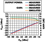
Fig. 12 Simulated and measured performance of the power amplifier.
Conclusion
A design methodology has been presented which facilitates the rapid prototyping and design of an RFIC by use of integrated foundry models, compliance test templates and links to test instruments. The design of a Bluetooth transceiver was described including simulated results and hardware verification performed under a unified EDA environment.
Acknowledgment
The authors wish to acknowledge the cooperation and support of Agilent Technologies and Taiwan Semiconductor Manufacturing Co. Ltd.
References
1. To learn more about the Bluetooth Design Guide or ADS2001, visit www.agilent.com/ eesof-eda.
2. Bluetooth SIG web site at: http://www. bluetooth.com/developer/specification/ specification.asp, December 1999.
Bob Koupal is manager of IC development and CAD at Signia Technologies. Prior to joining Signia, he was a custom EDA solutions architect at Agilent Technologies and managed R&D programs for Hewlett-Packard and Avantek. He holds an MSEE from Santa Clara University and a BSEE from the University of California at Davis.
Marshall Wang received his BS degree from National Taiwan University in 1982, and his MS and PhD degrees from Rensselaer Polytechnic Institute in 1987 and 1990, respectively. He jointed Hittite Microwave in 1990. From 1992 to 1994, he was the principal engineer in the IC Design Center of M/A-COM. From 1994 to 1996, Dr. Wang was one of the starting members and the team leader at Kokusai Electric America, a Hitachi affiliate. From 1997 to 1999, he joined Repeater Technologies as the director of engineering. Since November 1999, Dr. Wang has been with Signia Technologies as CTO and VP of engineering. He is also the co-founder of the company.
Cory Edelman is an applications engineer for Agilent EEsof EDA, specializing in communication system applications. He has over 21 years of industry experience, and for the past 13 years has been involved in the technical support, customer education and applications development of RF wireless systems simulations. He holds a BSEE from California State University at Northridge.