
Technical Feature
A Varactor-tuned Oscillator with Linear Tuning Characteristic
Munkyo Seo, Joo-Yeol Lee and Kyung-Kuk Lee
LG Electronics Inc.
Seoul, Korea
Sangwook Nam
Seoul National University
Seoul, Korea
In certain areas of microwave applications such as FMCW radars, FM modulators and phase-locked loop (PLL) circuits, the system performance is enhanced when the frequency of a voltage-controlled oscillator (VCO) is linear with respect to its control voltage.1,2 Although YIG-tuned oscillators have good linearity as well as a wide tuning range, their low tuning speed restricts their usefulness.1 Varactor-tuned oscillators (VTO), on the other hand, feature high speed tuning, although their linearity is inferior to that of YIG-tuned oscillators. Therefore, improving the linearity of VTOs has been the subject of much research. D. Peterson, for example, suggests a varactor doping profile3 which is capable of providing a wide band tuning linearity with series-tuned oscillator circuits. E. Marazzi, et al. use a CAD technique4 to optimize linearizing networks with predetermined topology. D. Kajfez5 utilized a pole-zero representation of lossless networks and a Taylor series technique in order to investigate the possibility of linear tuning. In some cases, external linearizers can be a solution, although they introduce new problems, such as additional power consumption, lower input impedance and narrower tuning bandwidth.7
In this article, a practical approach to the design of linear VTOs is presented, which focuses on the optimum selection of a varactor and the design of its coupling network. Since the tuning linearity of a VTO is mainly determined by the voltage-to-capacitance relationship of a varactor as well as its coupling network, the choice of a varactor and the design of a coupling network are critical to achieve the desired tuning linearity. Measurement results of two 4.3 GHz VTOs are also included as an example.

Fig. 1 General varactor-tuned oscillator schematic.
Derivation of a Simplified VTO Model
The schematic of a popularly used VTO is shown in Figure 1 .6 The capacitor at the emitter terminal, CE , forms a positive feedback loop together with the base-emitter diffusion capacitance of Q1. The negative resistance generated by Q1, which is needed to sustain a stable oscillation, can be controlled by varying CE .6 LRES , CS and CV (V) together act as an effective resonator whose reactance can be changed by controlling VTUNE . The coupling capacitor, CS , not only blocks the DC current flow between varactor and Q1, but also provides control over the tuning bandwidth.

Fig. 2 Equivalent circuit of packaged microwave bipolar transistors.
Fig. 3 Simplified VTO model.
Figure 2 is a general equivalent circuit of a packaged bipolar transistor, where the base-to-collector depletion capacitance is neglected for simplicity. If Rp > 1/wCp is assumed, which is valid at high frequency, Rp can also be neglected. After removing the bias circuitry and replacing Q1 by its equivalent circuit, a simple VTO model is obtained (as shown in Figure 3 ), where only the reactive elements that are responsible for the determination of the oscillation frequency are included. CT and LT are given by
CT = (CS -1 + Cp -1 + CE -1 )-1 (1)
LT = LRES + LBB + LEE (2)
Parasitic inductances, such as the via inductance and lead inductance of the varactor not considered here, may also be lumped into Equation 2, if their actual values are known or can be estimated. The varactor capacitance, CV (V), is a function of the control voltage, V, and can be expressed as
where
Cj0 = zero-bias junction capacitance
Vj = built-in junction potential
M = grading coefficient determined by the doping profile, generally ranging from 0.5 to 2
Design Procedure Considering Tuning Linearity
The resonant frequency of the simple VTO model is given as
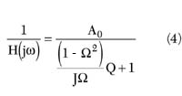
As shown in Equation 4, w0 (V) is a nonlinear function of V, and therefore, in general, the tuning curve will not be a perfectly straight line. First, two extreme cases are considered:
When

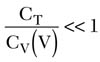
w0 (V) is approximated by
and thus the varactor capacitance solely determines the resonant frequency along with LT . This would be the limiting case for a wideband VTO, and using a hyperabrupt junction varactor with M=2 will result in a straight line.
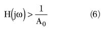
When
w0 (V) is approximately given by Equation 6 where a hyperabrupt junction varactor with M=1 will linearize the tuning curve.
In this case, the oscillation frequency is mainly determined by CT , which is much smaller than CV (V), resulting in a narrowband VTO.
In the general case between the two extremes just mentioned, the optimum grading coefficient, M, will be somewhere between 1 and 2, which means that a hyperabrupt junction varactor with M ≥ 1 is essential in order to achieve the best linearity in a VTO configuration. Also, Equation 4 shows that the tuning curve is completely specified by four circuit parameters, LT CT , CT /Cj0 , Vj and M, as long as the VTO model is correct. The design goals - center frequency, bandwidth and tuning linearity - should be met by adjusting these parameters. Although the number of design parameters is greater than the number of design goals, the actual design procedure is less flexible than it seems to be, since a circuit designer generally does not have individual control over Cj0 , Vj and M. These values become fixed once he chooses one from a list of available varactors.
LT CT and CT /Cj0 can be expressed in terms of the center frequency fc , the tuning bandwidth BW, Vj and M, by evaluating Equation 4 at the start and stop frequencies of oscillation. V1 and V2 are the start and stop tuning voltages, respectively
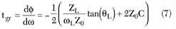
where

If the design requirement of fc and BW are given, Equation 7 allows an entire tuning curve with a specific varactor to be obtained by evaluating Equation 4 at several control voltages. In order to calculate the best-fit straight line (BSL) of an actual tuning curve, a general-purpose spreadsheet program might be useful. Actual values of Vj and M from datasheets can be used, or Vj may be fixed at some representative value, namely 2, and the calculations repeated with different values of M to find the optimum grading coefficient. After a proper varactor is chosen, CT and LT can be found from Equation 7, thus completing the first-pass design.
Fig. 4 The effect of varactor packaging capacitance on the tuning curve.
Until now, the varactor package capacitance, Cp, has been neglected. It is connected in parallel with the varactor. Although this capacitance is small, typically ranging from 0.1 to 0.2 pF, depending on the structure, it sometimes has a non-negligible effect on the linearity. In the high frequency region of the tuning curve, the varactor capacitance approaches its minimum and the package capacitance of the varactor sets a lower limit of the varactor total capacitance. This will, in turn, impose an upper limit on the tuning curve. Figure 4 illustrates this situation, together with the effect of CT , which establishes the lower limit of the oscillation frequency. The effect of CT will actually be compensated if the optimum M is selected by repetitively evaluating Equation 4, simply because it is a function of CT . The effect of CP , on the other hand, can be compensated with an additional inductive element (qV ) across the varactor, as shown in the overall RF schematic of Figure 5 . This inductance will make the slope of varactor reactance steeper as the frequency approaches the resonant frequency, thus shaping the tuning curve concave upward, as will be seen in the next section.
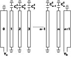
Fig. 5 Simplified RF equivalent circuit of a 4.3 GHz VTO.
Design and Measurement Results
Based on the procedure outlined in the previous section, a 4.3 GHz VTO was designed. The SPICE parameters of varactors under consideration are listed in Table 1 . With the design requirement of fc = 4.3 GHz and BW = 160 MHz, together with the listed varactor parameters, LT CT and CT /Cj0 were calculated using Equation 7 for each varactor. Next, the tuning curves were calculated with Equation 4, and their deviation from corresponding BSLs are shown in Figure 6 . Since this design belongs to a narrowband VTO whose fractional bandwidth is 3.7 percent, an optimum M close to 1 was expected. 1SV284(M = 1.03) yields the smallest deviation from a BSL and 1SV280(M = 0.981) gives the second best result. LT was calculated to be 3.9 and 7.88 nH, and CT was 0.37 and 0.185 pF for 1SV284 and 1SV280, respectively. LT = 3.9 nH will result in a very small value of LRES , since LT is the sum of all the inductances along the resonating path as shown by Equation 2. Therefore, 1SV280 was finally selected despite its slightly worse linearity than 1SV284, since, in this case, LT = 7.88 nH is a more desirable value.
|
Table 1 | |||||
|
Part No. |
Is |
BV |
Cj0 (pF) |
Vj |
M |
|
1SV280 |
5.38 10-16 |
15 |
6.89 |
3.272 |
0.981 |
|
1SV284 |
1.07 10-15 |
10 |
23.0 |
2.18 |
1.03 |
|
1SV285 |
4.17 10-16 |
10 |
6.9 |
2.6 |
1.3 |
|
1SV314 |
5.38 10-16 |
10 |
10.4 |
2.567 |
1.83 |
In the overall RF schematic, qS and qE are microstrip lines whose lengths are smaller than 1/4 l, and thus correspond to LRES and CE , respectively. CS is realized by a series connection of two 1005-size capacitors. qV cancels the varactor packaging capacitance, and can be controlled to further shape the tuning curve, if needed. It can be seen, in Figure 7 , that the curve becomes concave upward as qV becomes electrically shorter. The optimum qV is found to be approximately 50°. The AT-42086 bipolar transistor from Agilent was biased at 20 mA and its operating fT was approximately 7 GHz. To increase both isolation and output power, a Minicircuits ERA-5SM amplifier was cascaded. Its S21 at 4.3 GHz is about 14 dB with 60 mA of bias current. The output power at the main port is designed to be greater than 10 dBm. The coupled port can be used to provide a feedback signal in a PLL, or a downconverting LO in FMCW radars.
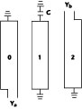
Fig. 6 Calculated deviations from a BSL.
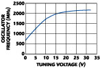
Fig. 7 The effect of q V in the tuning curve shape.
Two VTOs were implemented based on virtually the same design. Both VTOs share the same schematic, but one of them additionally employs an added tuning voltage shifter shown in Figure 8 . LM285D-1.2, an integrated zener diode from National Semiconductor, was used in this circuit. The shifter adds a constant offset voltage to the incoming tuning voltage in order to avoid a low bias region where junction rectification may occur due to the RF signal. This rectification is known to increase a post-tuning drift,3 and thus is undesirable. Another function of this shifter is to scale down the range of tuning voltage by a voltage divider formed by R3 and R2 . CS must be increased accordingly, since the actual range of tuning voltage applied to the varactor is reduced. The advantage with this simple shifter is that it offers another control over the tuning curve by carefully adjusting the amount of shifting and scaling.

Fig. 8 Tuning voltage shifter.

Fig. 9 Measured tuning curve of the VTO without tuning voltage shifter.

Fig. 10 Measured tuning curve of the VTO with tuning voltage shifter.
The measured electrical characteristics of the two VTOs are summarized in Table 2 . The shifter was adjusted to provide approximately 2.5 V of shifting and 0.7 of scaling down. A comparison of Figures 9 and 10 show that the VTO with a shifter has a better linearity with 1.32 MHz of maximum deviation from a BSL, compared with the VTO without a shifter, which has 3.83 MHz of maximum deviation. The price paid for this improvement of linearity is the higher phase noise due to the noise generated by the zener diode. Also, the input impedance at the tuning port is lowered, and the tuning speed will be slower due to the response time of the zener diode and the RC delay from the biasing resistors and diode capacitance. This delay will have to be carefully checked if the VTO is to be used in fast-switching applications.
|
Table 2 | ||
|
|
VTO |
VTO |
|
Power supply (V) |
15 | |
|
Current consumption (mA) |
20 for VCO only | |
|
Tuning voltage (V) |
0 to 10 | |
|
Center frequency (MHz) |
4271.3 |
4292.5 |
|
Tuning bandwidth (MHz) |
170.6 |
180.0 |
|
Output power @ center frequency (dBm) |
10.5 |
10.2 |
|
Power variation across entire band (dB) |
<1.4 |
<1.9 |
|
Maximum deviation from BSL (MHz) |
3.83 |
1.32 |
|
Average tuning sensitivity (MHz/V) |
16.45 |
17.84 |
|
Phase noise (100 kHz offset) (dBc/Hz) |
-104.4 |
-97.9 |
|
Second harmonic (dBc) |
-23.5 |
-28.5 |
|
Pushing factor (MHz/V) |
4.7 |
1.8 |
|
Pulling factor (12 dB return loss) (MHz) |
19.2 |
16.8 |
Conclusion
A design procedure has been proposed which emphasizes the tuning linearity of a VTO. If the center frequency and bandwidth requirements are given, LT CT and CT /Cj0 can be calculated using Equation 7 with the SPICE parameters of a specific varactor. Next, the entire tuning curve can be obtained with Equation 4, which gives the resonant frequency of the simplified VTO model. With the help of a spreadsheet program, a BSL and the deviation of an actual tuning curve from a BSL can be calculated. This procedure enables a designer to evaluate the tuning linearity prior to actual circuit design, and thus helps to select the optimum varactor. Based on this design procedure, two 4.3 GHz VTOs were designed, implemented and measured. The tuning linearity and ease of design were both considered in selecting the varactor. By using an inductive element parallel to the varactor, the shape of the tuning curve was further optimized. The maximum deviations from a BSL were measured to be 3.83 and 1.32 MHz for the VTOs with and without a tuning voltage shifter, respectively, verifying the usefulness of the proposed approach.
Acknowledgment
The authors would like to thank Mr. Jae-Hoon Lee for his help and discussion during the measurements.
References
1. P. Denniss and S.E. Gibbs, "Solid-state Linear FM/CW Radar Systems: Their Promise and Their Problems," IEEE S-MTT International Microwave Symposium Digest , 1974, pp. 340-342.
2. I.S. Kim, K. Jeong and J.K. Jeong, "Two Novel Radar Vehicle Detectors for the Replacement of a Conventional Loop Detector," Microwave Journal , Vol. 44, No. 7, July 2001, pp. 22-40.
3. D.F. Peterson, "Varactor Properties for Wide Band Linear-tuning Microwave VCOs," IEEE Transactions on Microwave Theory and Techniques , Vol. MTT-28, February 1980, pp. 110-119.
4. E. Marazzi and V. Rizzoli, "The Design of Linearizing Networks for High Power Varactor-tuned Frequency Modulator," IEEE Transactions on Microwave Theory and Techniques , Vol. MTT-28, July 1980, pp. 767-773.
5. D. Kajfez, "Linearity Limits of the Varactor-controlled Osc-mod Circuits," IEEE Transactions on Microwave and Techniques , Vol. MTT-33, July 1985, pp. 620-625.
6. Y.H. Kao and C.C. Chien, "Frequency Control in a Low Voltage, Wide Tuning VCO Design at 2.4 GHz," Microwave Journal , Vol. 44, No. 7, July 2001, pp. 128-140.
7. "Voltage-controlled Oscillators Evaluated for System Design," AN-M024, Agilent Technologies.
Munkyo Seo received his MS degree in electronic engineering from Seoul National University in 1996. Since 1997, he has been a research engineer at LG Electronics Inc., where he is involved with the design of RF subsystems for wireless communication.
Joo-Yeol Lee received his PhD degree in electrical engineering from Kwangwoon University, South Korea, in 1977. In 1997, he joined LG Electronics Inc., where he is a senior research engineer.
Kyung-Kuk Lee received his MS degree in electrical engineering from Hanyang University, South Korea. He is currently a research fellow at LG Electronics Inc.
Sangwook Nam received his PhD degree in electrical engineering from the University of Texas in 1989. Since 1990, he has been on the faculty at Seoul National University, where he is currently a professor in the school of electrical engineering.