
Cover Feature
A High Gain Power Amplifier with Variable Bias for Multi-mode WCMDA Applications
RF Micro Devices
Greensboro, NC
This article describes a new high performance power amplifier (PA) for wideband code division multiple access (WCDMA) applications. With the transition from second generation (2G) systems, such as Global System for Mobile Communications (GSM), to third generation (3G) wireless standards, such as WCDMA, several new PA requirements arise. The new requirements are discussed first from a system perspective and then from a circuit design perspective. Two new technologies that were chosen to meet the design goals are described.
GSM is currently the most widely used standard for mobile telephones and handsets. GSM was originally intended for voice communication and featured a limited data capability. Whether Web browsing, downloading e-mail or sending pictures, handset users are increasingly demanding phones with the ability to transmit data. As the number of data users and data services increases, higher data rates will be required. 3G mobile handset standards, such as WCDMA, have been specifically developed to cater to high data rate applications.
What Are the System Requirements for a WCDMA PA?
To accommodate higher data rates, a spectrally efficient modulation scheme is required. For the WCDMA uplink (handset to basestation) hybrid phase shift keying (HPSK) modulation has been selected. HPSK modulation has been chosen because it reduces the peak-to-average ratio over traditional modulation schemes such as quadrature phase shift keying (QPSK) or offset QPSK (OQPSK).1 For WCDMA, the peak-to-average ratio varies depending on the number of data channels being used by a handset. The higher the number of channels in use, the higher the peak-to-average ratio. With the maximum number of channels, and therefore highest data rate, WCDMA has a peak-to-average ratio of approximately 6 dB. Based on a 6 dB peak-to-average ratio, it is apparent that the power amplifier must be linear.
Power amplifier efficiency is an important parameter for any handset and WCDMA handsets are no exception. Most WCDMA handset users will be upgrading from GSM handsets that have PAs with power-added efficiencies (PAE) greater than 50 percent. GSM uses a form of phase modulation known as Gaussian minimum shift keying (GMSK), that operates with 0 dB peak-to-average, or alternatively, a constant envelope. Therefore, the PA in a GSM handset can be operated in a saturated mode, which makes PAEs of greater than 50 percent a realistic possibility. With a system linearity requirement of -33 dBc over temperature measured with a 5 MHz offset, a WCDMA PA must operate at a power level reduced from saturation. Operating in this "backed off" condition makes it extremely difficult for a WCDMA PA to achieve a PAE of 50 percent. In addition, limitations in the linearity of the remainder of the transmit chain (modulator) can force a more typical minimum requirement of -35 or -36 dBc. Achieving such a stringent linearity requirement generally forces a trade-off in PAE creating a decrease in radio talk time.
Currently, WCDMA PAs are measured based on maximum output power. A typical first generation WCDMA PA can achieve approximately 35 percent PAE. The target for the new RF3137 PA was greater than 40 percent at maximum rated output power.
First generation WCDMA products will be single-mode, meaning they will be capable of only operating in WCDMA mode. Single-mode phones will launch the first systems, and service is expected to be available only in large cities. The mass-market adoption of WCDMA will take place when multi-mode handsets become available. These handsets will include WCDMA and dual-band GSM operation. In large cities, where WCDMA networks exist, the phone will operate in WCDMA mode. In rural areas, the phone will operate in GSM mode. As a result, a dual-mode, tri-band phone will be required. The RF3137 PA featured in this article is intended for dual-mode phones and has the capability of being disabled with a logic signal.
The WCDMA specification is called Universal Mobile Telecommunications System (UMTS)2 and was developed by the Third Generation Partnership Project (3GPP). The standard specifies a range of output power classes with the most popular being Class 3 and Class 4. Class 3 requires an output power at the antenna of 24 dBm +1/-3 dB and Class 4 requires 21 dBm +/-2 dB. The new RF3137 is intended to meet Class 3 requirements.
To ensure that adjacent channels do not interfere with each other, the linearity requirements of the system must be met across all output power ranges of the handset. The adjacent channel leakage ratio (ACLR) linearity requirements are defined as
ACLR1 = -33 dBc at a 5 MHz offset
ACLR2 = -43 dBc at 10 MHz offset
Both are measured with a raised root cosine (RRC) filter, with a = 0.22, and a bandwidth equal to the chip rate, which is 3.84 MHz. As mentioned earlier, the PA must have additional ACLR margin over the system specification to allow for the contributions of the other blocks in the handset, such as the modulator. For WCDMA, a margin of 3 dB above system requirement is assumed to account for the contributions of the other blocks involved in the transmit chain.
Pre- and Post-power Amplifier Losses
A typical block diagram for second generation WCDMA handsets is shown in Figure 1 . The architecture is for a multi-mode WCDMA/ GSM/DCS handset. From the block diagram, it can be seen that the output signal from the WCDMA PA travels through an isolator (0.5 dB loss), a WCDMA duplexer (1.5 dB loss) and a switchplexer (1.5 dB loss) to reach the antenna. All post-PA losses are shown in parenthesis. This architecture contributes a maximum combined post-PA loss of 3.5 dB.

Fig. 1 Multi-mode WCDMA block diagram.
Before the PA, the typical input configuration would be a quadrature modulator feeding a driver amplifier and a surface acoustic wave (SAW) filter. A typical driver amplifier has a maximum drive in the range of 8 dBm at room temperature and approximately 5 dBm at temperature extremes. A typical SAW filter has a loss of approximately 2.5 to 3 dB.
This system level block diagram produces the following formulae that describes the required capability of the power amplifier:
PIN_MAX = PDRIVER_MAX - (SAW filter loss)
PIN_MAX = +5 dBm - 3 dB = +2 dBm
POUT_MAX = (Class 3 power) + (total post-PA loss)
POUT_MAX = 24 dBm + 3.5 dB = 27.5 dBm
GainMIN is then calculated as
GainMIN = POUT_MAX - PIN_MAX
+ gain margin
= 27.5 dBm - 2 dBm + 2 dB
= 27.5 dB
Noise Power Considerations
Receive band noise power is the power that the PA outputs at the receive frequencies. This power interferes with the downlink signal in the handset's receiver or in an adjacent handset. For multi-mode handsets, the receive band noise must be specified at both the WCDMA receive band and the GSM900 and GSM1800 bands. The most difficult requirement for receive band noise is the frequency band from 1805 to 1880 MHz. This band is almost adjacent to the transmit band of 1920 to 1980 MHz; therefore, the switchplexer and duplexer provide negligible rejection for the PA energy in this band. The system specification requires -71 dBm/100 kHz for the noise at the antenna in the 1805 to 1880 MHz band. This translates to -121 dBm/Hz, and, once margin is added to ensure the PA is not the limiting block, the requirement is -130 dBm/Hz. Table 1 presents a basic PA specification based on fundamental system requirements.
|
Table 1 | ||||
|
Parameter |
Minimum |
Typical |
Maximum |
Conditions |
|
Gain (dB) |
27.5 |
29 |
31 |
over extremes |
|
ACLR (dBc) |
36 |
38 |
|
5 MHz offset, over extremes |
|
ACLR (dBc) |
46 |
50 |
|
10 MHz offset, over extremes of voltage and temperature |
|
Noise power (dBm/Hz) |
|
|
-143 -130 -150 |
2110 to 2170 MHz |
Design Considerations
To determine the correct architecture when designing a PA, a trade-off must be made among a number of parameters. The most fundamental trade-off when designing a linear power amplifier is determining whether the amplifier should have two or three stages. With a linear application, such as WCDMA, design engineers must consider three parameters: efficiency, gain and receive band noise. Current two-stage amplifiers for WCDMA have gain of approximately 25 dB at room temperature, rolling off to around 22 dB at temperature extremes. As can be seen from previously sited system requirements, this is not enough gain for future WCDMA systems. Typically, designers would consider a three-stage amplifier to meet the gain requirement.
A three-stage amplifier can produce a typical gain of 30 dB, which easily meets the system requirement. One of the disadvantages of a three-stage amplifier, however, is that it has three cascaded stages, which creates poor receive band noise. A typical three-stage amplifier has noise power of approximately -137 dBm/Hz, while a typical two-stage amplifier has only -144 dBm/Hz. The extra gain stage causes higher cascaded noise figure and higher out-of-band gain. The cascaded noise figure formulas for both two-stage and three-stage amplifiers are
NF (3 Stage) = NF1 + (NF2 -1)/G1 + (NF3 -1)/(G1 ·G2 )
NF (2 Stage) = NF1 + (NF2 -1)/G1
The term (NF3 -1)/(G1 ·G2 ) is the term that introduces additional noise.
Relative to the in-band gain, a three-stage amplifier tends to have more out-of-band gain than a two-stage amplifier. The additional gain in the receive band amplifies the noise by a greater amount at the input. The extra gain is a side effect of having three stages in the PA. For WCDMA applications, the gain from a three-stage PA is excessive. The gain must be rolled off with feedback and interstage matching. It is fundamentally hard to remove all gain due to the lower Q interstage matching associated with the reduced impedance transform ratio required with a three-stage versus a two-stage.
The optimum solution for a WCDMA PA appears to be a two-stage amplifier with improved gain. The requirement for high efficiency, low receive band noise and high gain has led to the development of the RF3137 in a new high gain semiconductor process.
Temperature Performance
Mobile phone manufacturers are becoming increasingly concerned with the performance of their handsets at temperature extremes. A typical operating temperature range for a mobile phone is -30° to +85°C. This extended temperature range presents a number of challenges for a typical two-stage power amplifier. All BJT devices have a negative slope associated with b with respect to temperature. As temperature increases, b and gain decrease. Conversely, as the PA gets colder, b and gain increase. The device b slope equates to significant gain variation as a function of temperature. Figure 2 shows gain vs. temperature for a three-stage amplifier that has some temperature compensation, which reduces the current and gain as the temperature is lowered.

Fig. 2 Typical three-stage amplifier gain vs. temperature at Vcc =3.4V and VREG =2.8 V.
At the same time, the VBE of the heterojunction bipolar transistor (HBT) devices has a slope-over-temperature of approximately -1.3mV/°C. The result is a variation in the idle current of the amplifier over temperature. The resulting idle current variation can increase the AB hump at low temperatures and affect the linearity.
It would be ideal to keep the idle current and gain constant over temperature. The variation in these temperature-dependent parameters will lead directly to the requirement of an increase in the margin for both the gain and linearity at room temperature. Linearity and efficiency are the normal trade-offs made through changes to the resistive part of the load line presented to the PA. As the required linearity margin is reduced, it is possible to improve the efficiency even further.
Circuit Solutions
Bias Control Circuit
It is desirable to keep the idle or quiescent current of the power amplifier constant over temperature. The same is true for variations in the power supply voltage, wafer processing, component values and any other variations that may be introduced.
The RF3137 PA uses a unique, closed loop bias control scheme. As shown in Figure 3 , the loop is comprised of a silicon CMOS power amplifier control chip, the GaAs PA and a minimum number of passive components. The function of the control chip is to maintain an accurate quiescent current when variations are encountered and to provide an interface between the GaAs PA and the external control signals that are sent to the module.
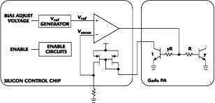
Fig. 3 Bias control loop for each stage of the PA.
The quiescent current of the PA and the corresponding RF performance is set by providing an analog voltage to the input of the CMOS power control chip. The input voltage is translated into a reference voltage that is used for comparison in the closed loop feedback circuit.
Each stage of the power amplifier has a sense circuit that provides a small current as feedback to the power control chip. The current is an accurate representation of the quiescent current of that stage. The current flows through a current mirror and is fed into a resistor to establish a sense voltage. The sense voltage is compared against the reference voltage via an operational amplifier. The operational amplifier adjusts the input to the PA until the reference voltage and sense voltage match.
The accuracy of each control loop is limited mainly by the value of the sense resistor and any small mismatch between the sense current and quiescent current of the stage. In order to minimize the error introduced by the value of the sense resistor, precision off-chip resistors have been used. Other contributors of slight inaccuracies are random offsets in the operational amplifier, the finite gain of the feedback loop and variations in the reference voltage.
As mentioned earlier, the RF3137 was designed with the intention that it could be utilized in a multi-mode phone. Therefore, an enable function was included, which allows the PA to be toggled off-and-on via a digital logic signal.
Process Technology
The company's new HBT process leverages the low cost and high yield of its standard process, which has been in high volume production for more than five years.3 However, to optimize HBT performance for power amplifier applications, some features in the device structure have been changed. These changes were designed to improve the RF gain of the device and improve the uniformity of b over temperature and current density.
Most of the improvements in the new HBT are in the epitaxial layers that are grown by molecular beam epitaxy (MBE). Therefore, the fabrication steps for the new process are almost identical to the previous process, allowing the company to take advantage of a well-established manufacturing capability while improving device performance. Process features include 2 mm minimum emitter sizes, two levels of metal interconnect, a thin-film resistor, high and low density metal-insulator-metal (MIM) capacitors, wafer thinning, through-substrate vias and a backside metallization.
|
|
|
|
Fig. 4 Normalized b vs. temperature. |
Fig. 5 b vs. collector current density. |


The improvement in b performance over temperature is shown in Figure 4 . b for both processes is normalized to 30°C values. For the old process, b drops by more than 40 percent from 30° to 120°C. For the new process, b drops by less than 20 percent over the same temperature range. This improved temperature performance reduces the gain and idle current variation of the PA.
There is a similar improvement in the b vs. current relationship, as shown in Figure 5 . b is normalized to 20 kA/cm2 values. Between 0.1 and 20 kA/cm2 , b increases by 2X for the new process and by more than 3X for the standard process. As a result, there is less gain and linearity variation with bias current variation.
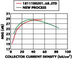
Figure 6 compares maximum stable gain (MSG) versus current density for an 80 mm2 device at 1900 MHz and VCE = 1.7 V. In the 10 to 30 kA range, which is the typical operating current density, there is more than 1 dB improvement in MSG from the standard process to the new process. As a result, enough gain has been realized in a two-stage amplifier to produce 27.5 dBm output power (Class 3) with 0 dBm drive level.
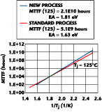
To verify the reliability of the new process technology, a standard three-temperature accelerated life test was performed. The results of the test are shown in the Arrhenius plot in Figure 7 . This data indicates that the mean time to failure (MTTF) estimate for the new process is similar to that estimated for the standard process, and the two processes have comparable reliability.4
|
|
|
|
Fig. 6 MSG at 1.9 GHz vs. collector current density at VCE =1.7 V. |
Fig. 7 Comparison of three-temperature life test data. |
Amplifier Performance
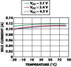
The RF3137 PA features a built-in bias loop designed to provide a constant quiescent current across temperature and supply voltage variations. The variation is within 12 percent of the nominal value at room temperature and 3.4 V.
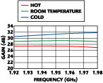
Because of the nearly constant quiescent current, the PA maintains its high gain even at extreme temperatures. The quiescent current variation for different temperatures and supply voltages is shown in Figure 8 and Figure 9 shows the gain over frequency and temperature variations. The required gain of 27 dB is maintained over temperature. This is remarkable for a two-stage power amplifier and clearly demonstrates the high gain that can be achieved with the 3G process.
|
|
|
|
Fig. 8 Quiescent current vs. temperature. |
Fig. 9 Gain vs. frequency and temperature. |
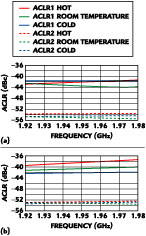
The main challenge for a WCDMA power amplifier is meeting the linearity requirements over the full supply voltage and temperature range. Figure 10 shows the ACLR for different supply voltages and temperatures. Although there is degradation in performance when going from 3.4 to 3.1 V, the requirement of -36 dBc is met over the full temperature range with no back-off from the 27.5 dBm output power.
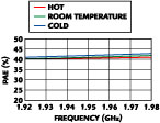
Figure 11 shows the PAE of the amplifier vs. frequency and temperature. The PAE is taken at an output power of 27.5 dBm and a supply voltage of 3.4 V. A minimum efficiency of 40 percent is seen at all frequencies and temperatures. The noise performance of the RF3137 PA is a key advantage over existing PAs. At full output power the noise specifications, listed in the table of performance requirements, are met with 3 dB of margin.
|
|
|
|
Fig. 10 ACLR vs. frequency at Vcc =(a) 3.4 V and (b) 3.1 V. |
Fig. 11 PAE vs. frequency. |
The noise performance margin allows us to relax the TX filter requirements. With only modest requirements on out-of-band filtering, a low TX insertion loss is possible. Since the TX filter loss is a major contributor to the overall efficiency, by reducing insertion loss, system efficiency is improved. The good noise performance of the RF3137 PA underlines the benefits of using a two-stage PA for WCDMA.
Conclusion
New 3G cellular handset standards are placing rigorous new requirements on PA designers. The most difficult challenge is to meet all of the system requirements over the temperature and supply range of a typical handset. Two new technologies have been introduced that include enhancing the standard GaAs HBT process and implementing a bias controller to produce a two-stage PA with greater than -40 dBc ACPR and 40 percent efficiency across all conditions. The RF3137 PA was designed for manufacturability, and the choice of technology and bias method makes this part extremely repeatable. The new power amplifier demonstrates how careful system analysis and technology matching can produce a superior performing solution.
References
1. K. Laird, N Whinnett and Soodesh Buljore, "A Peak-to-average Power Reduction Method for Third Generation CDMA Reverse Links," IEEE, 1999.
2. Universal Mobile Telecommunications System (UMTS); UE Radio Transmission and Reception (FDD), (3GPP TS 25.101 version 4.1.0 Release 4), ETSI TS 125 101, version 4.1.0 (2001-06) ETSI.
3. A. Geissberger, et al., "Transfer and Qualification of a Layout-compatible Second Source HBT Technology for Mobile Phone Applications," 1999 International Conference on GaAs Manufacturing Technology Digest , Vancouver, BC, Canada, April 19 - 22, 1999.
4. M. Fresina, et al., "Reliable AlGaAs/GaAs HBTs Grown by MBE with Increased Beryllium Doping and Aluminum Concentration," Presented at the 2001 IEEE GaAs Reliability Workshop , Baltimore, MD, October 21, 2001.
RF Micro Devices Greensboro, NC (336) 664-1233 www.rfmd.com
Circle No. 300