
Technical Feature
A Broadband, Four-bit, Ka-band MMIC Phase Shifter
A compact, robust and broadband, four-bit, Ka-band phase shifter was designed and fabricated in a standard 0.25 mm PHEMT GaAs process. Design trade-offs, simulation versus measured results and architectures for the various bits to achieve broadband performance are discussed. Electro-magnetic (EM) and linear analyses combined with measurements of the first pass design are used to refine a second pass fabrication, which includes a potential future fifth bit. Based on first pass results, a second pass four-bit phase shifter was designed to operate from 28 to 36 GHz with 8 ±1 dB of insertion loss.
John E. Penn
Johns Hopkins University Applied Physics Laboratory (APL)
Laurel, MD
Increasing carrier frequencies in communications systems offer greater data transmission rates. Changing from X-band (8 GHz) to Ka-band (32 GHz) has the potential for a sixteen fold improvement in data rates for a given antenna size and transmitter power. In deep space missions, where the available DC power is limited, improving the amount of data returned in a given mission is of great interest.
The phase shifter is a key component in a phased array system. Changing the phase of each array element allows the main antenna beam to be steered towards the receiver system. The original application for this four-bit phase shifter is a deep space communications array, but its general-purpose, broadband design makes it useful for many other systems.
The design trade-offs for the phase shifter are insertion loss, insertion balance between phase states and phase accuracy. Size is a criterion but may not be as important as performance in the intended application.
Each bit of phase shift uses a topology or circuit architecture appropriate for that particular phase shift. A topology that works well for large phase shifts may be inappropriate or inefficient for small phase shifts. Parasitic capacitances in the switches must be compensated for, or incorporated into, the phase shifter topology. Several topologies were explored for each of the 4 phase shift bits - 180°, 90°, 45° and 22.5°.
Designing at Ka-band frequencies, especially regarding phase, is much harder than at lower frequencies. An error in line length amounting to 5° at X-band (8 GHz) becomes a 20° error at Ka-band (32 GHz). Modeling errors in the switch devices, microstrip or MMIC components accumulate quickly. Switching devices are far from ideal at Ka-band. Rather than use exotic GaAs processing techniques to reduce the effects of parasitic capacitances in the switch elements1 , a standard PHEMT process is used, with phase shift architectures chosen to absorb the parasitics for broadband operation. Careful analysis of linear and EM simulations in combination with measured results produced an improved second pass four-bit design that is compact, broadband and has good insertion loss and balance, yet uses a standard 0.25 mm PHEMT process with standard bias voltages.
PHEMT Switches
|
|
|
Fig. 1 Modified six-element PHEMT switch model. |

Switching elements are made from 0.25 mm PHEMT devices fabricated in TriQuint's GaAs process. The two states of a switch are ON, usually defined by a gate bias of 0V, and OFF, usually defined by a gate bias of at least 2 to 4 times the pinchoff voltage of the device. Small signal operation of the phase shifter is desired to minimize distortion. An ideal switch should toggle between a short circuit and an open circuit. In reality, a PHEMT switch looks like a resistance in the ON state and a parasitic capacitance in the OFF state. The larger the device, the smaller the ON state resistance. Unfortunately, the OFF state capacitance should be very small, necessitating a small device, which conflicts with the previous requirement. This OFF state capacitance must be compensated for, particularly at Ka-band. It can be absorbed or incorporated into the phase shifter topology, or it can be compensated for with an inductance, which may lead to a design with a narrow band response.
The total switch size (periphery) is obtained from the number of FET fingers multiplied by the width of each individual finger. For example, a 300 mm device could be made of four 75 mm fingers or six 50 mm fingers. To a first order, the resistances in the model vary proportionally to the total FET periphery, while the capacitances vary inversely. Inductances, to a first order, tend to be proportional to the FET finger width, but inversely proportional to the number of FET fingers. A simple switch model would be a single resistor for the ON state and a single capacitor for the OFF state. A more accurate switch model can be obtained with a six-element model using 3 resistors and 3 capacitors plus inductances for the gate, drain and source (Figure 1 ).2 A six-element switch model for the PHEMTs is provided in the TriQuint foundry manual,3 optimized for a 300 mm device. The rules for scaling the inductances in the switch model are somewhat confusing. The errors increase as one scales the switch model away from its nominal size, but determining the quantitative error is difficult. For EM simulations, it can be difficult to incorporate a realistic physical switch model. For initial EM and linear simulations, the simple single resistor/single capacitor switch model is very useful.
For EM simulations, how much of the FET physical structure must be included in the model needs to be considered. The interconnect could be simulated by EM and then combined with the standard six-element model for high level linear simulations. One simple EM switch model may include the metallization for the drain and source feeds with a simple thin film resistor to model the ON state resistance, and a simple dielectric plate capacitor to model the OFF state capacitance. For this design, it appeared that EM simulating the simple ON resistor/OFF capacitor of the physical FET model with the interconnect worked well.
Lange Coupler
|
|
|
Fig. 2 Switched line/reflection 180° bit. |

Lange couplers are not often used in MMICs because their quarter wave (l/4) length size can be quite large. At Ka-band frequencies and above, quarter wave size components can reasonably fit on a MMIC. For the intended space communications application, performance is more important than GaAs die size. Using Agilent EEsof's Libra simulator and Linecalc program, the coupler's line width, line spacing and overall length was chosen. Additional simulations with Ansoft HFSS and Sonnet showed agreement in the Lange coupler's length, but not its line width and spacing. HFSS was in close agreement to EEsof, so its length and spacing predictions were used for the layout over Sonnet's predictions. Measurements were not available on individual Lange couplers to determine the optimal spacing for the desired 3 dB split, but, based on the phase shifter performance, the initial Lange coupler design seems to be sufficient.
180° Line/Reflected Bit
For large phase shifts, a broadband switched line/reflected bit topology is used (Figure 2 ). A Lange coupler connected to substrate vias provides a relatively broadband 180° phase shift. Switching between a l/4 line and an equal length Lange coupler shorted to ground provides a broadband 180° phase difference. Tuning inductances at each PHEMT compensate for the switch's OFF state capacitances.
|
|
|
|
Fig. 3 Measured and simulated first pass phase vs. frequency response of 180° bit. |
Fig. 4 Measured and simulated second pass phase vs. frequency response of 180° bit. |


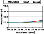
Initially, the linear simulator Libra was used for the first pass design. EM simulations with Ansoft HFSS and Sonnet were used for analysis of the first design and for designing a second pass four-bit phase shifter design. While the first pass 180° bit had reasonable insertion balance, the phase flatness was not as broadband as expected. Figure 3 shows the measured phase of the first pass 180° bit versus linear and EM simulations. Attempts to improve the 180° phase flatness using linear and EM simulations seemed to decrease the bandwidth of the design or to increase the insertion balance mismatch. Since the first pass 180° bit worked reasonably well, only a minor change was made to center the 180° phase shift from 28 GHz in the initial design to 32 GHz while retaining good insertion balance. Figure 4 shows the phase shift of the second pass "slightly retuned" 180° bit.
90° Reflected Bit
|
|
|
Fig. 5 Measured and simulated second pass phase vs. frequency response of 90° bit. |

The original 90° bit used a switched line/reflected bit topology similar to the 180° bit, but with significantly different component values. PHEMTs used for switching between the two "states" of the 90° bit varied in size by an order of magnitude. EM simulations of the 90° bit showed a dramatic difference from the linear simulations. However, the EM simulations did not match the measured results very well for the first pass 90° bit. The EM simulator qualitatively predicted a problem in the switched line path that was evident in the measurements. One potential source of error is in scaling the switch model for devices that deviate considerably from the 300 mm size to which the models are fit. The switched line path that modeled poorly used a relatively small 82 mm PHEMT switch. However, the alternate path using a 528 mm PHEMT agreed well with linear and EM simulations.
In the second pass design, the 90° bit was redesigned with a reflected bit topology as opposed to the switched line/reflected bit topology. While the insertion balance mismatch for the reflected bit topology increases with increased phase shift, this topology was expected to produce a 90° bit with relatively low design risk. The insertion balance mismatch could be projected from the first pass results of the 22° and 45° bits to be approximately 0.7 dB for the new 90° bit. Figure 5 shows the measured second pass 90° bit versus the linear and EM predictions. Some additional retuning should improve and flatten the 90° phase response.
45°/22.5° Reflected Bit
|
|
|
Fig. 6 Broadband reflection 45° bit. |

For moderate phase shifts, a broadband reflected bit topology is used (Figure 6 ). A Lange coupler attached to a tuned switching element provides the phase shift. Each reflected bit consists of a PHEMT switch, a capacitor and a tuned inductor. The values are optimized to provide a broadband phase shift while minimizing insertion loss and maintaining insertion balance between the phase states.
Ideally, all the RF energy would be reflected at the coupled ports of the Lange coupler to the isolated port forming the through path of the phase shifter bit. The PHEMT size is primarily chosen for phase shift differential with a trade-off for insertion balance. A larger PHEMT switch tends to improve the insertion balance while reducing the differential phase shift. The values of the inductors, capacitors and PHEMTs are selected by optimizing the trade-offs between bandwidth, insertion loss and insertion balance.
|
|
|
Fig. 7 Measured and simulated second pass phase vs. frequency response of 45° bit. |

The Lange coupler in this reflected bit topology provides a broadband match due to the symmetry of the loads. As mentioned previously, the success of the first pass reflected bit designs led to a new 90° bit.
Both the 45° and 22° reflected bit topologies differed from EM and linear simulations by as much as 20°. For the redesigns, the EM and linear simulators were used only for qualitative predictions. Figure 7 shows second pass results showing the excellent phase response of the 45° bit from 20 to 40 GHz. A second pass 22.5° reflected bit design was included as a test structure in the second pass MMIC and appears to need another design adjustment.
22.5°/11.25° High Pass/Low Pass Bit
For small phase shifts, a high pass/ low pass bit topology is used (Figure 8 ). High pass/low pass networks work well in MMICs since they tend to be small in size and are broadband. There are many topologies for high pass/low pass networks. The better ones absorb the parasitic capacitances of the switches by incorporating them as elements in the high pass/low pass architecture. Larger phase shift amounts tend to require more elements (that is, complexity). While the differential phase shift tends to be broadband for this topology, it can be difficult to balance the insertion loss between states.
|
|
|
|
Fig. 8 High pass/low pass 22.5° bit. |
Fig. 9 Measured and simulated second pass phase vs. frequency response of 22.5° bit. |

For the 22° and 11° phase shifts, a simple topology was chosen which provides broadband performance in a compact size. In the first phase shifter design, there were two 22.5° bit topologies - a reflected bit and a high pass/low pass bit. The first high pass/low pass 22.5° phase shifter worked so well and was so compact that it was incorporated in the new four-bit phase shifter design. The only minor modification to the high pass/low pass 22.5° bit was the addition of a 1 to 2 kW bias resistor from the PHEMT drain to ground to avoid a floating bias potential. Results were virtually identical for the two fabrications of the 22.5° bit (within measurement error). Figure 9 shows the simulated phase of the 22.5° bit versus measured results.
In the second pass fabrication, an 11° high pass/low pass bit was designed and added for possible future use in a five-bit Ka-band phase shifter. While the phase shift was indeed approximately 11° at 32 GHz, the phase response was not as broadband as expected and the insertion loss was much higher than expected - 4 dB measured versus 1 dB expected. If GaAs area is available in a future five-bit design, a reflected bit topology would probably be preferred over this 11° bit.
Layout
|
|
|
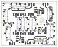
Fig. 10 120 mil x 150 mil dual four-bit Ka-band phase shifter. |
The relatively inexpensive Prototype Chip Option for TriQuint's 0.25 mm PHEMT process was used for fabricating the original four-bit phase shifter. A 100 x 120 mil die contained the four-bit phase shifter, an additional high pass/low pass 22.5° bit and one test bit from each of the reflected bit (22.5°) and switched bit (180°) topologies. Some additional test structures were included to evaluate the 22.5° and 45° reflected bit designs.
The second pass layout with two complete four-bit paths and individual test bits used a larger 120 x 150 mil GaAs die, as shown in Figure 10 . All individual bit designs were included as test structures on the second pass layout except for the marginally retuned 180° bit.
Measured Results
Measurements of the first pass test bits and four-bit phase shifter were compared to linear (Libra) and EM (Sonnet) simulations. Since there are modeling issues for the switches, microstrip and other MMIC elements that lead to errors, measurements were used in conjunction with linear and EM simulations to redesign the phase shifter. The new design is a 120 mil x 150 mil chip using the TriQuint 0.25 mm PHEMT Prototype Chip Option that contains two four-bit phase shifters and test structures. Since the 180° bit has the narrowest bandwidth, one four-bit shifter has a 180° bit centered at 32 GHz (28 to 36 GHz) and another, nearly identical four-bit shifter has a modified 180° bit centered near 28 GHz (24 to 32 GHz). Changes from the first pass design include a very slightly modified 180° bit, a completely redesigned 90° bit using the reflected bit topology, a slightly re-tuned 45° bit and an unchanged high pass/low pass 22.5° bit replacing the previous reflected 22.5° bit topology.
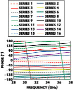
Some cabling changes to the probe station improved measurements in the 30 to 40 GHz range, but the probe heads used were limited to 40 GHz. Some of the designs could have benefited from measurements above 40 GHz to determine their true bandwidth potential. Figures 11 and 12 show the overall insertion loss and phase for all sixteen states of the broadband four-bit phase shifter.
|
|
|
|
Fig. 11 Measured insertion loss of four-bit Ka-band phase shifter for all 16 states. |
Fig. 12 Measured phase shifter of the four-bit Ka-band phase shifter for all 16 states. |

Conclusion
A broadband four-bit GaAs phase shifter at Ka-band frequencies has been designed, fabricated, measured and analyzed. Linear versus EM simulation issues and modeling of the PHEMT switches have been explored. It is very difficult to achieve accurate phase predictions at Ka-band, which makes two (or more) fabrication cycles almost essential for success. Measurements of the first pass must be used as a base for redesigning a second pass MMIC. Broadbanding of the phase shifter bits not only makes the final design useful in more systems, but it increases the tolerance of the design to GaAs processing variations. While the intended application of this phase shifter was a deep space mission, its broadband operation makes it applicable to LMDS communications, radar, satellite communications and other Ka-band systems. This Ka-band phase shifter MMIC uses a standard commercial 0.25 mm PHEMT process from TriQuint allowing for easy reproducibility and manufacture. The author is not aware of any current commercially available Ka-band phase shifter MMICs of comparable performance.
Acknowledgment
The author wishes to acknowledge the assistance of his coworkers, particularly Craig Moore, Perry Malouf, Sheng Cheng, Bob Wallis and Lloyd Ellis. Many people at TriQuint Texas were very helpful, such as foundry manager Lisa Howard and the engineers involved in a three-day foundry course at the TriQuint Texas facilities in February of 2000. NASA funded initial development of the Ka-band phase shifter MMICs under GSFC contract NAS5-97271, task order 14, Advanced Technology Development (ATD).
References
1. K. Maruhashi, H. Mixutani and K. Ohata, "Design and Performance of a Ka-band Monolithic Phase Shifter Utilizing Nonresonant FET Switches," IEEE Transactions on Microwave Theory and Techniques , Vol. MTT-48, No. 8, August 2000, pp. 1313-1317.
2. R. Goyal, Monolithic Microwave Integrated Circuits: Technology & Desig n, Artech House Inc., Norwood, MA, 1989, p. 500.
3. TriQuint Texas Foundry Design Manual , Rev. 5.1, 1999.
4. M.J. Schindler and M.E. Miller, "A Three- bit K/Ka-band MMIC Phase Shifter," IEEE 1988 Microwave and Millimeter-wave MMIC Symposium , pp. 95-98.
5. C. F. Campbell and S. A. Brown, "A Compact Five-bit Phase-shifter MMIC for Satellite Communication Systems," IEEE Transactions on Microwave Theory and Techniques , Vol. MTT-48, No. 12, December 2000, pp. 2652-2656.
6. B. Pillans, S. Eshelman, A. Malczewski, J. Ehmke and C. Goldsmith, "Ka-band RF MEMS Phase Shifters for Phased Array Applications," 2000 IEEE RFIC Symposium , pp. 195-198.
7. M. Soulard, M. Delmond, J. Cazaux, Y. Laporte, J. Sarkissian and J. Villemazet, "Evolution and Recent Development in MMICs for Space Application," 2000 2nd International Conference on Microwave and Millimeter-wave Technology Proceedings , pp. 219-222.
8. T. Takagi, K. Yamauchi, Y. Itoh, M. Komaru, Y. Mitsui, H. Nakaguro and Y. Kazekami, "MMIC Development for Millimeter-wave Space Application," Microwave Conference, 2000 Asia-Pacific , pp. 658-663.