
Technical Feature
A Broadband Planar Isolator Using Coupled Microstrip Lines on a Magnetized Gyrotropic Substrate
A new type of broadband isolator, using coupled microstrip lines on a transversely magnetized gyrotropic substrate, is proposed in this article. The nonreciprocal coupling between two microstrip lines can be used to create an isolation mechanism. Based on this phenomenon, an isolator is designed at 20 GHz, which has an 8 GHz bandwidth with more than 15 dB isolation and less than 2.1 dB insertion loss.
Y.C. Moon
KMW Inc.
Korea
J.R. Lee, S.W. Yun and I.S. Chang
Sogang University
Dept. of Electronic Engineering
Seoul, Korea
Gyrotropic materials have been widely used in nonreciprocal devices such as isolators, circulators and phase shifters at microwave as well as millimeter-wave frequencies. However, the majority of such devices are usually fabricated using waveguides or striplines. Several authors have proposed planar isolators based on field displacement inside the ferrite substrate.1,2 Such isolators must use absorbers to suppress the backward wave propagation, even though they present a broad bandwidth. When a nonreciprocal coupling mechanism3 is used, the power reflected back toward the generator is absorbed by a 50 W load which can be placed inside or outside the device. This mechanism is conducive to high power applications. In this article, a planar type broadband isolator, based on nonreciprocal coupling between two microstrip lines on a magnetized gyrotropic substrate, is proposed.
Even though many authors have analyzed nonreciprocal wave propagation on magnetized substrates,4-9 their main interest concentrates on the nonreciprocity itself, rather than new nonreciprocal devices. In 1994, Lindell, et al.10 proposed a theory for nonreciprocal transmission lines on layered structures of bi-isotropic media, but this theory is not applicable to transmission lines on magnetized gyrotropic substrates whose magnetic properties are represented by a permeability tensor.
Here, using the nonreciprocal propagation characteristics obtained from coupled microstrip lines on a transversely magnetized ferrite substrate, a new type of isolator is presented. For an effective design, the trends of nonreciprocity functions of variations of dimensional parameters and bias magnetic field strength are investigated. In order to create an isolation mechanism, the nonreciprocal transmission line equations, including the nonreciprocal characteristics as a function of the wave direction propagation, are expanded from the conventional transmission line equations.11,12 The nonreciprocal multi-port impedance and scattering parameters are derived. It is also shown that an isolator can be designed by properly choosing the length of the coupled lines.
Fig. 1 Cross-section of multiple coupled microstrip
lines on a multilayer substrate, including a
gyrotropic layer.
Analysis
The cross-section of the shielded multiple coupled microstrip lines under consideration is shown in Figure 1 together with the coordinate system. The transversely magnetized gyrotropic substrate is located between two lossless dielectric layers. This structure is assumed to be uniform and infinite in the z direction. It is also assumed that the conductor strips are lossless and have a negligible thickness. The direction of the wave propagation lies in the z-axis. When an external biasing magnetic field is applied in the x direction, the tensor permeability of the gyrotropic substrate is expressed as
with

where
f = operating frequency
g = gyromagnetic ratio
H0 = applied biasing magnetic field
4pMs = saturation magnetization of the gyrotropic substrate
|
|
|
|
Fig. 2 Normalized phase constant of the coupled microstrip lines as a function of frequency and applied magnetic field. |
Fig. 3 Characteristic impedance of the coupled microstrip lines as a function of frequency and applied magnetic field. |
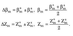
A spectral domain approach is used to compute the phase constants for the dominant modes.11,12 Symmetrically coupled microstrip lines (w1 = w2 = 0.9 mm, s = 0.8 mm) are analyzed, where a magnetized layer (4pMs = 1750 G, Ho = 4300Oe, e2 = 12.2 e0 , d = 1.0 mm) as well as dielectric layers (e1 = e3 = e4 = e0 , l1 = h = 0.0 mm, l4 = 10 mm) are enclosed within a rectangular conductor box (a = 30 mm, b = 11 mm). Figure 2 shows the normalized phase constant (b/ko ) in the absence of an external magnetic field, and the separation of the phase constants as a function of the direction of propagation when an external magnetic field bias is applied (Ho = 4300Oe). The forward wave (Fw) represents the wave propagating along the +z direction and the backward wave (Bw) along the -z axis. Figure 3 shows the characteristic impedance as a function of frequency, in which the characteristic impedances are also different depending on the direction of the wave propagation when the biasing magnetic field is applied. However, the difference is very small compared with the differential phase shift. The differential phase shift Db/ko is expressed as
where
b+ and b- = phase constants along the ±z propagation directions, respectively
Because the differential phase shift reflects the nonreciprocal effects, its variations as a function of dimensional parameters and external magnetic field intensity are also calculated and compared at 20 GHz. Figure 4 shows the differential phase shift as a function of the thickness of the gyrotropic layer d. The differential phase shifts of the two modes increase as the thickness d increases. However, the two curves show a saturation above a certain thickness. The differential phase shifts for the two modes increase with increasing bias magnetic field Ho , as shown in Figure 5 .
|
|
|
|
|
|
Fig. 4 Differential phase shift as a function of the ferrite substrate thickness. |
Fig. 5 Differential phase shifter as a function of applied magnetic field. |
Fig. 6 Differential phase shift as a function of the microstrip width. |
Fig. 7 Differential phase shift as a function of the gap dimension. |
The differential phase shift as a function of the symmetrical coupled line structure dimensions, strip width w = w1 = w2 and gap s = s1 = s2 have also been calculated. Figure 6 shows that the differential phase shift for the odd-mode is maximum at a certain strip width, while that of the even-mode decreases as the strip width w increases. The differential phase shift versus the gap between the strips is shown in Figure 7 . That of the even-mode decreases as the gap increases, while that of the odd-mode is maximum at a certain gap s.
From these results, it can be deduced that a fairly large nonreciprocity will be achieved with variations of dimensional parameters and biasing magnetic field strength.
Network Parameters of Nonreciprocal Transmission Lines
|
|
|
Fig. 8 Diagram of a single nonreciprocal transmission line. |
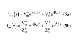
For a single nonreciprocal transmission line, shown in Figure 8 , the transmission line equations, including the nonreciprocal characteristics depending on the direction of the wave propagation, are expanded from the conventional transmission line equations10 as
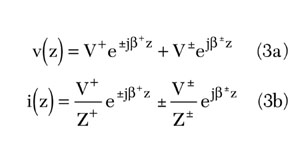
where
b+ and b- = phase constants for each direction of the wave propagation (±z axis)
Z+ and Z- = characteristic impedances for each direction of the wave propagation (±z axis)
The impedance matrix, derived from the relations between voltage and current at z = -l and z = 0, is obtained as
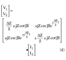
with

By comparison to a section of ordinary line, there is notable difference from the magnetized ferrite nonreciprocity, Z12 = -Z*12 , Z11 = -Z*22 . It is easily seen that the impedance matrix in Equation 4 becomes that of an ordinary transmission line if Db = DZ = 0.
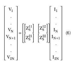
For a N-coupled transmission line, a 2N x 2N impedance matrix was derived by H.Y. Yang.8 The N-coupled transmission line equations are defined as
where
b+m and b-m = phase constants depending on the direction of the wave propagation for the mth mode
Z+m and Z-m = characteristic impedances depending on the direction of the wave propagation for the mth mode
|
|
|
Fig. 9 Relations between port voltages and currents and mode voltages and currents. |
Rearranging the N-coupled transmission lines into a 2N-port network, the mode voltages and currents are replaced with port voltages and currents. The voltage eigenvector relates between mode voltages and port voltages, as the current eigenvector does. These relations between modes and ports are described by using ideal transformers, as shown in Figure 9 . From these relations together with Equation 5, the 2N-port impedance matrix of the N-coupled transmission line is given by
with

and
The subscript "diag" in the above submatrices |Zs ij | indicates a diagonal matrix. The 2N-port scattering matrix, referred to Zo , is obtained from the impedance matrix in Equation 6.
|
Table 1 | |||
|
|
No Bias (H0 = 0) |
Biased (H0 = 4300Oe) | |
|
Forward Wave |
Backward Wave | ||
|
b/k0 |
3.1357 |
3.1453 |
2.9976 |
|
Characteristic impedance (W) |
54.335 |
54.201 |
52.171 |
|
Impedance parameter (W) |
Z11 =Z22 =-j50.16 |
Z11 =Z*22 =1.015+j1903.3 | |
|
Scattering parameter (S) |
S11 =S22 =0.061L 42.60 |
S11 =0.0023L -88.40 | |
|
Table 2 | ||||
|
|
Forward Wave |
Backward Wave | ||
|
Even-Mode |
Odd-Mode |
Even-Mode |
Odd-Mode | |
|
b/k0 |
3.2662 |
2.9417 |
3.1701 |
2.6933 |
|
Current eigenvector (MI ) |
0.70711 |
0.70711 |
0.70711 |
0.70711 |
|
Characteristic impedance (W) |
63.082 |
41.004 |
61.237 |
37.128 |
|
Impedance parameter (W) |
Z11 =Z22 =-Z33 *=-Z44 *=1430+j84.556 | |||
|
Scattering parameter (S) |
S11 =S22 =0.095L -6.81 |
S31 =S42 =0.546L -23.52 | ||
The two-port impedance and scattering matrices of a single transmission line of strip width w = 0.9 mm and length l = 31.7 mm at 20 GHz are given in Table 1 . The phase difference between S12 and S21 is 112.43° (237.82° - 125.39°) when the gyrotropic layer is magnetized, and this differential phase shift is caused by the nonreciprocity of the magnetic substrate. In Table 2 , the same parameters for four-port impedance and scattering matrices at 20 GHz are listed for a line length l = 31.7 mm.
Isolator Design
|
|
|
Fig. 10 Isolator using nonreciprocal coupled transmission lines. |
Figure 10 shows the two-port nonreciprocal-coupled microstrip lines that have b+e,o , Z+e,o for the forward wave and b-e,o , Z-e,o for the backward wave. In this case, the even- and odd-modes of the coupled microstrip line have the differential phase shifts.
According to Equation 7, the nonreciprocal coupled microstrip lines can be used as an isolator. If the nonreciprocal coupling length is adjusted to a value where the incident power at one port is coupled to the other line, while in the reverse excitation the incident power is not delivered to the other line, an isolation mechanism takes place.
Because of the nonreciprocity of the magnetized gyrotropic layer, the even- and odd-modes of the coupled microstrip lines have differential phase shifts as shown in previous sections. Therefore, the electrical lengths of the coupled lines are changed as the direction of the wave propagation is reversed. If the coupling length is adjusted in such a way that the incident power at one port is coupled to the other line, while for the reverse excitation the incident power is not delivered to the other line, an isolation mechanism takes place.13 By using this phenomenon, an isolator at 20 GHz was designed. The isolator was designed for a ferrite substrate with a relative dielectric constant of 12.2, a 4pMs = 1750G, a size of 50 x 30 mm and a thickness of 1 mm. The dielectric layer dimensions are h = 0.0 mm, l1 = 0.0 mm and l4 = 10 mm with dielectric constants eo (air). The structure is shielded with a rectangular conductor box (a = 30 mm, b = 11 mm). The strip widths and gap are chosen as w1 = w2 = 0.9 mm and s = 0.8 mm for impedance matching to the reference impedance of Zo = 50 W.
|
|
|
|
Fig. 11 Magnitude of the S-parameters of the two-part coupled line structure as a function of coupling length. |
Fig. 12 Frequency response of the designed isolator. |
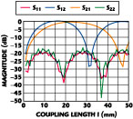

The magnitude of the two-port scattering parameters as a function of the coupling length l creates the isolation mechanism. As shown in Figure 11 , |S21 | and |S12 | vary as the coupling length l increases and an isolation greater than 20 dB is obtained for coupling lengths l = 31.7 mm and 46.6 mm. The design with the shortest length (which gives an insertion loss of about 2 dB) has been chosen. Material and radiation losses are not considered in the design.
Once the coupling length is chosen, the two-port scattering parameters are calculated, as shown in Figure 12 . The designed isolator shows an 8 GHz bandwidth with more than 15 dB isolation, less than 2 dB insertion loss and less than -15 dB return loss. The bandwidth of this type of isolator is limited at the upper frequency by the dispersion characteristics of the microstrip lines and at the lower frequency by the propagation of magnetostatic waves.
Conclusion
A new type of broadband isolator applicable at millimeter-wave frequencies has been proposed. This new device uses the nonreciprocal coupling between two microstrip lines fabricated on a magnetized gyrotropic substrate. The simulated results at 20 GHz are presented. They show that the nonreciprocal coupling between two microstrip lines on a ferrite substrate can offer the characteristics of an isolator. Since an external 50W load can be used to absorb the reflected power, high power applications are possible.
References
1. M.E. Hines, "Reciprocal and Nonreciprocal Modes of Propagation in Ferrite Stripline and Microstrip Devices," IEEE Transactions on Microwave Theory and Techniques , Vol. MTT-19, May 1971, pp. 442-451.
2. A. Beyer and K. Solbach, "A New Finline Ferrite Isolator for Integrated Millimeter-wave Circuits," IEEE Transactions on Microwave Theory and Techniques , Vol. MTT-29, December 1981, pp. 1344-1348.
3. S.W. Yun and T. Itoh, "A Novel Millimeter-wave Isolator," Proceedings of the 13th European Microwave Conference , Nuremburg, September 1983, pp. 174-178.
4. Y. Hayashi and R. Mittra, "An Analytical Investigation of Finlines With Magnetized Ferrite Substrate," IEEE Transactions on Microwave Theory and Techniques , Vol. MTT-31, June 1983, pp. 495-498.
5. M. Geshiro and T. Itoh, "Analysis of Double-layered Finlines Containing a Magnetized Ferrite," IEEE Transactions on Microwave Theory and Techniques , Vol. MTT-35, December 1987, pp. 1377-1381.
6. C.M. Krowne, "Fourier Transformed Matrix Method of Finding Propagation Characteristics of Complex Anisotropic Layered Media," IEEE Transactions on Microwave Theory and Techniques , Vol. MTT-32, December 1984, pp. 1617-1625.
7. M. Tsutsumi and T. Asahara, "Microstrip Lines Using Yttrium Iron Garnet Film," IEEE Transactions on Microwave Theory and Techniques , Vol. MTT-38, October 1990, pp. 1461-1467.
8. Hung-Yu Yang, "Microstrip Open-end Discontinuity on a Nonreciprocal Ferrite Substrate," IEEE Transactions on Microwave Theory and Techniques , Vol. MTT-42, January 1994, pp. 2423-2428.
9. T. Kitazawa, "Nonreciprocity of Phase Constants, Characteristic Impedances and Conductor Losses in Planar Transmission Lines With Layered Anisotropic Media," IEEE Transactions on Microwave Theory and Techniques , Vol. MTT-43, February 1995, pp. 445-451.
10. I.V. Lindell, M.E. Valtonen and A.H. Sihvola, "Theory of Nonreciprocal and Nonsymmetric Uniform Transmission Lines," IEEE Transactions on Microwave Theory and Techniques , Vol. MTT-42, February 1994, pp. 291-297.
11. V.K. Tripathi and H. Lee, "Spectral-domain Computation of Characteristic Impedances and Multiport Parameters of Multiple Coupled Microstrip Lines," IEEE Transactions on Microwave Theory and Techniques , Vol. MTT-37, January 1989, pp. 215-221.
12. Y.C. Moon, S.W. Yun and I.S. Chang, "Analysis of Multiple Coupled Microstrip Lines on a Magnetized Ferrite Substrate," Journal of KITE , Vol. 33-A, No. 5, May 1996, pp. 65-74.
13. S.W. Yun and T. Itoh, "Nonreciprocal Wave Propagation in a Hollow Image Guide With a Ferrite Layer," IEEE Proceedings , Vol. 132, Pt. H, No. 4, July 1985, pp. 222-226.
Y.C. Moon received his BS, MS and PhD degrees, all in electronic engineering, from Sogang University, Seoul, South Korea. From 1996 to 2000 he worked for ETRI. Since 2000 he has been working with KMW Inc. His principal research interest is RF circuit design.
J.R. Lee received his BS degree in physics and his MS degree in electronic engineering from Sogang University, Seoul, South Korea. From 1996 to 1998 he worked for Samsung Electro-Mechanics Co. Since 1998 he has been pursuing his PhD in electronic engineering from Sogang University. His principal research is in microwave and millimeter-wave circuit design.
S.W. Yun received his BS and MS degrees in electronic engineering from Seoul National University, Seoul, South Korea, and his PhD from the University of Texas at Austin. Since 1984 he has been a professor in the department of electronic engineering, Sogang University, Seoul, South Korea. From January to December 1988 he was a visiting professor at the University of Texas at Austin. His principal research is in microwave and millimeter-wave circuit design.
I.S. Chang received his BS, MS and PhD degrees, all in electronic engineering, from Seoul National University, Seoul, South Korea. From 1969 to 1971 he worked in the Research Center of the Korean Ministry of Communication. From 1971 to 1974 he served as a full-time instructor at the Korean Military Academy. Since 1974 he has been a professor in the department of electronic engineering, Sogang University, Seoul, South Korea. From September 1982 to August 1983 he was a visiting professor at the University of Wisconsin at Madison. His principal research is in RF circuit design.