
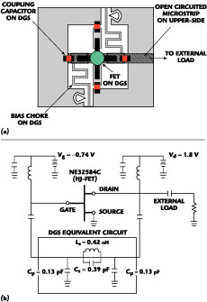
Technical Feature
Implementation of a Neural Network HEMT Model into ADS
Neural network algorithms have been applied to various areas of engineering and computer science. A high electron-mobility transistor (HEMT) large-signal model has been implemented in the Advanced Design System (ADS) software package using a multilayered neural network. The neural network model was trained to the drain current, gate-source capacitance and gate-drain capacitance characteristics of an Angelov model previously developed. Training was done using the back-propagation algorithm, which achieved excellent results for the model. Linear and harmonic balance simulations were performed to compare the linear and power performance of the neural network model to the Angelov model, without any additional optimization after the initial training.
Willie L. Thompson II, Eric V. Miller and Carl White
Morgan State University Center of Microwave, Satellite and RF Engineering
Baltimore, MD
In recent years, device characterization and modeling have become essential components of the design cycle. Many CAD packages allow engineers to simulate and modify their circuits during the initial design cycle, which help to decrease the need for additional iterations and decrease the time-to-market, especially for microwave monolithic integrated circuits (MMIC). For accurate design simulations, engineers require device models for the active and passive components used in the CAD packages. These models must be accurate, reliable, easily extracted and have limited computational requirements.
Currently, there are several types of device models. Physics-based models (PBM)1,2 utilize solid-state physics equations to obtain the device characteristics. PBMs are very computer intensive, and, in some cases, the accuracy of the model is affected by assumptions made to solve closed-form equations. In addition, most PBMs are device dependent, which means a PBM of a HEMT device will not model the behavior of a metal-oxide semiconductor field-effect transistor (MOSFET) without modification of the model's equations. Empirical-based models (EBM)3-6 use multidimensional polynomials to simulate the device characteristics. Polynomial expressions provide good approximation for mild nonlinear characteristics, but usually breakdown for high nonlinearities such as DC characteristics at pinch-off. The empirical approach usually requires intensive extraction procedures following several measurements to obtain an accurate model. Table-based models (TBM)7 use a table of measured data to model the device characteristics. The size of the table grows at an exponential rate as the number of elements being modeled increases. In addition, TBMs require interpolation or extrapolation functions to obtain results at points that are not included within the range of the table's measurements, thus degrading the model accuracy. One major advantage of EBMs and TBMs is that they are less computer intensive than PBMs.
Neural networks (NN) have been reported for device and circuit modeling.8-10 A neural network is a mathematical approach for mimicking the way the human brain is able to learn and process data. The brain is a network of neurons that are connected to each other through axons. By modifying the axons or connections between the neurons in response to input data, the brain is able to learn the data. Using its neurons and axons, the brain is able to generate a representation of the data that can be used later in response to similar input data. Neural network algorithms use this same principle to learn data using a network of mathematical functions (neurons) and weights (axons) to generate a representation of the data. The major advantages of NN models are: theoretically, they can handle any degree of nonlinearity within the data;8 the size of the model does not increase exponentially with an increase in the number of characteristics being modeled; and the computational requirement is limited to the one time training of the NN model, which is usually performed off-line.
|
|
|
|
Fig. 1 Multilayered structure used from implementation of the NN model. |
Fig. 2 A typical large-signal HEMT equivalent circuit. |
A typical multilayered neural network is shown in Figure 1 , consisting of an input layer, hidden layer and output layer. Using a similar NN structure, Zaabab, et al.,8,9 have demonstrated NN algorithms used to predict device I-V curves and S-parameters with excellent results. Also, Shirakawa, et al.,10 have used NN algorithms to model the large-signal behavior for a HEMT. They have demonstrated good results for modeling Cgs and gm versus bias.
This article presents an approach for implementing a NN algorithm to develop a large-signal HEMT model to be used in ADS by circuit designers. A typical large-signal model is shown in Figure 2 . The NN model proposed in this article implements NN algorithms for Ids , Cgs and Cgd , with Ids being the most nonlinear element in the circuit, and Cgs and Cgd being secondary nonlinear elements that affect the accuracy of the model as suggested by Statz, et al.4 Using the Angelov model6 that was developed for a PHEMT device to generate the Ids , Cgs and Cgd data, the NN model was trained using the back-propagation algorithm. After training was completed, a set of weights for the NN structure was generated that represents the behavior of the elements in the model. After the weights set is imported into a user-defined ADS model, any simulation and results can be performed without the need of any additional optimization to the model. In particular, linear and harmonic balance simulations were performed to compare the S-parameters, maximum available gain, k-factor, power at 1dB compression point and power-added efficiency of the NN model with the Angelov model.
Multilayered Neural Network
Neural Network Structure
A typical multilayered NN structure consists of an input layer, hidden layer and output layer. Each circle represents a neuron with I neurons for the input layer, J neurons for the hidden layer and K neurons for the output layer. The hidden layer allows the NN to model the complex nonlinear relationship of the input and output efficiently and accurately. The network can have as many hidden layers as needed.
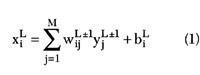
In this work, the model utilizes a three-layer NN structure. The total weighted input and output for the ith neuron in the L layers is given by
and
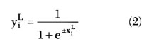
where M = number of neurons in the (L-1)th layer
The other parameters are defined in a sidebar on page 75. The size of the model does not grow exponentially when the number of input parameters is increased. The total number of model parameters is {(I x J) + (K x J) + (I + J + K)}. The first term is equal to the number of weights between the input layer and hidden layer, the second term is equal to the number of weights between the hidden layer and output layer, and the third term is equal to the number of bias weights for each neuron in the network. The input parameters for the model are Vgs and Vds with the output parameters being Ids , Cgs and Cgd .
Back-propagation Algorithm
The back-propagation algorithm is a popular training algorithm that minimizes the error between the outputs of the NN and desired outputs of the training set. The total error is given by
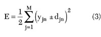
where
M = number of neurons in output layer
n = loop counter that indicates the current iteration of the training points, which ranges from 1 to the maximum number of training points
The main goal of the back-propagation algorithm is to adjust the weights and biases of the neurons to minimize the total error of the outputs. They are adjusted using

where
n = loop counter as shown previously
The training algorithm that was implemented for the model was based on the gradient descent method.9,11 The important structure and training parameters of the network are given in Table 1 .
|
Table 1 | |
|
NN layers |
3 |
|
Neurons in input layer, I |
2 |
|
Neurons in hidden layer, J |
75 |
|
Neurons in output layer, K |
3 |
|
Learning rate of weights, b |
0.01 |
|
Learning rate of biases, h |
0.1 |
|
Momentum term, a |
0.4 |
Angelov Empirical-based Model
Angelov6 describes a large-signal EBM for HEMT and MESFET devices. The model is capable of simulating the DC characteristics and capacitances of the device. The drain-source current is modeled using a harmonic series, while the derivatives of the current with respect to the potentials are modeled using singular-value decomposition. In addition, the model is capable of simulating Cgs and Cgd , which increases the model's accuracy in predicting the different harmonics.11 The empirical equations are
Ids = Ipk (1 + l Vds ) {1 + tanh (Y)}tanh(d Vds ) (6)
where
Ipk = drain current at maximum gm
l = channel length modulation
d = saturation voltage parameter
Y = P1 (Vgs - Vpk ) + P2 (Vgs - Vpk )2 + P3 (Vgs - Vpk )3 + ...
Pi = fitting coefficients
Vpk = gate voltage at peak gm
Cgs = Cgso {1 + tanh(f1 )}{1 + tanh(f2 )} (7)
Cgd = Cgdo {1 + tanh(f3 )}{1 + tanh(f4 )} (8)
where
f1 = P0gsg + P1gsg Vgs + P2gsg V2 gs + ...
f2 = P0gsd + P1gsd Vds + P2gsd V2 ds + ...
f3 = P0gdg + P1gdg Vgs + P2gdg V2 gs + ...
f4 = P0gdd + (P1gdd + P1cc Vgs )Vds + P0gdd V2 ds + ...
The term P1cc Vgs Vds reflects the cross coupling of Cgd with Vgs and Vds potentials. The remaining terms are fitting parameters.
An Angelov EBM was developed for a 600 mm NEC device (NEC-12801).11 The device was fully characterized from measured S-parameters with Vgs ranging from pinch-off to saturation (-2.0 to 0.2 V) and Vds ranging from 0 to 8 V, over a frequency range from 45 MHz to 26.5 GHz. DC measurements were taken for Ids , Igd and Igs . Upon measurement of the device S-parameters, a small-signal equivalent model was created for the bias points to obtain the intrinsic parameters. The Cgs and Cgd values, obtained from the small-signal models as a function of bias, were then fitted to satisfy Equations 7 and 8. The drain-source current was then fitted to the Angelov current Equation 6, while Igd and Igs were fitted to normal diode I-V expressions. The model parameters for Angelov's expressions are given in Table 2 . Good results for DC characteristics and S-parameters were demonstrated.11
|
|
|
|
|
Fig. 3 Comparison of the neural network output to training data for Ids . |
Fig. 4 Comparison of the neural network output to training data for Cgs . |
Fig. 5 Comparison of the neural network output to training data for Cgd . |
Training Results
For this work, the training data was obtained using the Angelov model that was described previously. The training data was generated directly for the NN model for Ids , Cgs and Cgd . Figures 3 to 5 are samples of training results for Ids , Cgs and Cgd , respectively. The training for the NN model was performed using a 166 MHz computer with a training time of 150 minutes. The training ranges for each output are shown in Table 3 . The training ranges are large for the first iteration of the model. More optimized data set size can be achieved, but was not the focus of this work.
|
Table 2 | |
|
Drain current at max. gm, Ipk |
0.24 |
|
Channel length modulation, l |
-0.03 |
|
Saturation voltage, d |
3.9 |
|
Ids fitting coefficient, P1 |
0.47 |
|
Ids fitting coefficient, P2 |
0.5 |
|
Ids fitting coefficient, P3 |
0.4 |
|
Gate voltage at peak gm, Vpk |
0 |
|
Capacitance parameter, Cgs o |
6.97e-13 |
|
Cgs fitting coefficient, P0gsg |
4.45 |
|
Cgs fitting coefficient, P1gsg |
2.56 |
|
Cgs fitting coefficient, P2gsg |
0 |
|
Cgs fitting coefficient, P0gsd |
-0.77 |
|
Cgs fitting coefficient, P1gsd |
0.02 |
|
Cgs fitting coefficient, P2gsd |
0 |
|
Capacitance parameter, Cgdo |
2.13e-14 |
|
Cgd fitting coefficient, P0gdg |
2.29 |
|
Cgd fitting coefficient, P1gdg |
1.43 |
|
Cgd fitting coefficient, P2gdg |
0 |
|
Cgd fitting coefficient, P0gdd |
0.38 |
|
Cgd fitting coefficient, P1gdd |
-0.34 |
|
Cgd fitting coefficient, P3gdd |
0 |
|
Cgd coupling coefficient, P1cc |
0 |
Implementation
The implementation of a NN model into ADS requires the development of a user-defined model. The three main steps in developing a user-defined model are:
1. Defining the parameters that the user will interface with the model from the ADS schematic.
2. Defining the circuit symbol and number of pins for interfacing with ADS simulators.
3. Development of C code.
|
|
|
Fig. 6 Implementation of the neural network into the circuit simulator |
The first two steps consist of developing the application extension language (AEL) code to interface the model with ADS. AEL provides the coupling of the model's parameters and pins in the schematic design to the simulator. The C code is used to define the device's response to its parameter configuration, simulation controls and pin voltages.
ADS has several types of simulators in which a model can be used. The linear simulator is used for emulating the small-signal response versus frequency of a transistor. Typical outputs include S-parameters, stability factor and maximum available gain. A small-signal or a large-signal model can be used within the linear simulator. The nonlinear simulator (harmonic balance) is used for the large-signal response of a transistor at different power excitations. The transient simulator is used to model the response of a transistor versus time. The harmonic balance and transient simulators require a large-signal model which accurately represents the behavior of a transistor.
In developing the user-defined model, the typical large-signal equivalent circuit is divided into a linear subnetwork and a nonlinear subnetwork. The linear subnetwork includes Ri , Rc , Rs , Rg , Rd , Crf , Cds , Ls , Lg and Ld , whose values can be obtained from extraction procedures and small-signal modeling. The linear elements do not exhibit bias dependence, but exhibit frequency dependence. The nonlinear subnetwork includes Ids , Igs , Idg , Cgs and Cgd , which exhibit strong bias dependence.
The implementation of a NN subnetwork into a harmonic balance simulator proceeds as follows. In a harmonic balance simulation, the simulator solves the harmonic balance equation
F(V) = I(V) + jWQ(V) + YV + Iss = 0 (9)
where
I(V) = currents out of the nonlinear subnetwork
Q(V) = charges out of the nonlinear subnetwork
Y = admittance matrix of the linear subnetwork
V = node voltages in the circuit
W = angular frequency matrix
Iss = sources
Zaabab, et al.9 proposed dividing the equivalent circuit into three subnetworks, which include the linear elements, the NN algorithm that is used to model to nonlinear relationship of the current and capacitances and all other nonlinear elements of the equivalent circuit as demonstrated in Figure 6 . The new harmonic balance equation is
F(V) = I(V) + jWQ(V)+ In (V) + jWQn (V) + YV + Iss = 0 (10)
where
In (V) = nonlinear NN current
Qn (V) = charges of NN capacitances
The NN subnetwork is simply included as an additional nonlinear subnetwork within the harmonic balance equation.
The NN user-defined model code contains three main functions that correspond to the linear subnetwork, nonlinear subnetwork and NN subnetwork. The linear function models the linear elements of the circuit and computes the admittance matrix, Y of Equation 10, for each node. The nonlinear function models the Igs , Idg . These two nonlinear current sources were fitted to normal diode I-V expressions as previously mentioned. This function computes the nonlinear I(V) and Q(V) matrices for Equation 10. Finally, the NN function models the Ids , Cgs and Cgd , and computes the nonlinear In (V) and Qn (V) matrices for Equation 10. In addition to providing the currents and charges, the nonlinear and NN functions must provide the derivatives of the currents and charges with respect to each voltage source. These derivatives are used in the linear simulator and enhance the convergence of the nonlinear simulator.
For this work, the NN algorithm was trained to the drain current, gate-source capacitance and gate-drain capacitance as discussed previously using data generated by an Angelov model. Once the off-line training was performed, the generated weight set is imported and used by the NN function within the ADS user-defined model. The charges for the subnetwork are generated from the capacitances and the current derivatives are computed. The linear and nonlinear functions remained the same as those used for the Angelov user-defined model with the same values for the elements, excluding the nonlinear elements modeled by the NN subnetwork.
|
|
|
|
Fig. 7 DC simulation results within training range. |
Fig. 8 DC simulation results for expanded range of Vgs and Vds . |
Verification
DC Simulations
DC characteristics are essential for the modeling of the linear and nonlinear performance of the transistor. DC characteristics within the training range of the neural network were simulated. Excellent DC performance of the NN model and the ability of the NN algorithm to predict untrained Vgs curves are demonstrated in Figure 7 . The untrained curves are Vgs = 0.15, -0.35, -0.85 and -1.35 V, respectively. Figure 8 demonstrates the DC characteristics exceeding the training range of the drain current. Once again, good DC performance of the NN model and the ability of the NN algorithm to predict untrained Vgs curves are demonstrated.
|
|
|
Fig. 9 S-parameters for Vgs =-0.95 V and Vds =5.0 V. |
Linear Simulations
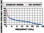
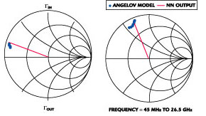
Linear simulations were performed to verify the small-signal analysis of the NN model to the Angelov model. S-parameter simulation results are demonstrated for a frequency range of 45 MHz to 26.5 GHz at a bias point of Vgs = -0.95 V and Vds = 5.0 V, as shown in Figure 9 . Maximum available gain, stability factor, and simultaneous-matched input gamma and output gamma were simulated. They are excellent indicators of the accuracy of the model to small-signal analysis.12 Excellent results are demonstrated in Figures 10, 11 and 12 . In addition to verifying the small-signal analysis of the model, performing linear simulations with a nonlinear large-signal model verify the convergence of the model to the small-signal case.
|
|
|
|
|
Fig. 10 Maximum available gain for Vgs =-0.95 V and Vds-5.0 V. |
Fig. 11 Stability factor for Vgs =-0.95 V and Vds -5.0 V. |
Fig. 12 Simultaneous-matched input/output gamma for Vgs =-0.95 V and Vds =5.0 V. |
Nonlinear Simulations
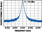
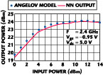
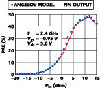
Nonlinear performance of the NN model was simulated using ADS's harmonic balance simulator. The harmonic balance simulation requires accurate modeling of the charge and capacitance at each node, and the derivatives of the drain current, which are used in Equation 10. The simulations were performed at a fundamental frequency of 2.4 GHz and a bias point of Vgs = -0.95 V and Vds = 5.0 V. Good output power versus input power characteristics are demonstrated in Figure 13 , with the power characteristics at the 1dB compression point (P1dB) given in Table 4 . The NN model predicted greater compression (or less output power) than the Angelov model, but the result is within 2 percent of the Angelov model. The power-added efficiency (PAE) versus input power is shown in Figure 14 and shows good agreement with the Angelov model.
|
|
| |||||||||||||||||||||||||||
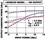
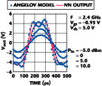
A large-signal model must model the harmonics that can be generated during nonlinear operation. The output power levels of the first three harmonics are demonstrated in Figure 15 . This simulation demonstrates the NN model's ability to model the different harmonics and shows good agreement with the Angelov model. The generation of harmonics will cause distortion of the output waveform as demonstrated in Figure 16 .
|
|
|
|
|
|
Fig. 13 Output power vs. input power. |
Fig. 14 PAE vs. input power. |
Fig. 15 Output power for the first three harmonics. |
Fig. 16 Output waveform vs. different input power. |
Conclusion
A nonlinear large-signal multilayered NN model implemented into Agilent's ADS is described. The model is fully integrated into the simulator, allowing any simulation to be performed with the model (DC, linear, harmonic balance and transient). The NN was trained to the drain current, gate-source capacitance and gate-drain capacitance off-line using a back-propagation algorithm. After training, the weight set of the NN was imported into ADS where no additional optimization was required to the model. Harmonic balance results of the model strongly agreed with the Angelov model. To the author's knowledge, this is the first reported fully integrated NN model in a commercially available CAD package demonstrating excellent linear and nonlinear results.
Acknowledgment
The authors would like to thank the Maryland Industrial Partnerships (MIPS) for funding of this work. The authors would also like to thank Marek Mierzwinski of Agilent Technologies, EEsof EDA Division, Kreative Control Systems Inc. (KCS) and to Adrian Gilbert of Hughes Space and Communications. Thanks also to the undergraduate research students of COMSARE (John Brice, Chris Guisto, Clifton Martin, Jerhome Petway and Ammyanna Williams).
References
1. J.W. Bandler, R.M. Biernacki, Q. Cai, S.H. Chen, S. Ye and Q.J. Zhang, "Integrated Physics-oriented Statistical Modeling, Simulation and Optimization," IEEE Transactions on Microwave Theory and Techniques , Vol. 40, 1992, pp. 1374-1400.
2. D.E. Stoneking, G.L. Bilbro, P.A. Gilmore, R.J. Trew and C.T. Kelley, "Yield Optimization Using a GaAs Process Simulator Coupled to a Physical Device Model," IEEE Transactions on Microwave Theory and Techniques , Vol. 40, 1992, pp. 1353-1363.
3. W.R. Curtice and M. Ettenberg, "A Nonlinear GaAs FET Model for Use in the Design of Output Circuits for Power Amplifiers," IEEE Transactions on Microwave Theory and Techniques , Vol. 33, 1985, pp. 1383-1394.
4. H. Statz, P. Newman, I.W. Smith, R.A. Pucel and H. Haus, "GaAs FET Device and Circuit Simulation in SPICE," IEEE Transactions on Electron Devices , Vol. 34, 1987, pp. 160-166.
5. S. Maas and D. Neilson, "Modeling of MESFETs for Intermodulation Analysis of Mixers and Amplifiers," 1990 IEEE MTT-S Digest , pp. 1291-1294.
6. I. Angelov, H. Zirath and N. Rorsman, "A New Empirical Nonlinear Model for HEMT and MESFET Devices," IEEE Transactions on Microwave Theory and Techniques , Vol. 40, 1992, pp. 2258-2266.
7. D.E. Root, S. Fan and J. Meyer, "Technology Independent Large-signal Non-quasistatic FET Models by Direct Construction from Automatically Characterized Device Data," Proceedings of the 21st European Microwave Conference , Stuttgart, Germany, September 1991, pp. 927-932.
8. A.H. Zaabab, Q.J. Zhang and M. Nakhla, "Analysis and Optimization of Microwave Circuits and Devices Using Neural Network Models," IEEE International Microwave Symposium Digest , San Diego, CA, 1994, pp. 393-396.
9. A.H. Zaabab, Q.J. Zhang and M. Nakhla, "A Neural Network Modeling Approach to Circuit Optimization and Statistical Design," IEEE Transactions on Microwave Theory and Techniques , Vol. 43, 1995, pp. 1349-1358.
10. K. Shirakawa, M. Shimiz, N. Oktubo and Y. Daido, "A Large-signal Characterization of an HEMT Using a Multilayered Neural Network," IEEE Transactions on Microwave Theory and Techniques , Vol. 45, 1997, pp. 1630-1633.
11. A. Gilbert and C. White, "Implementing a Bias Dependent Large-signal Into a Well Known Circuit Simulator," Morgan State University, 1996.
12. C. Giusto and C. White, "Techniques for Small-signal Modeling," Applied Microwave and Wireless Magazine , May 2000, pp. 42-46.