
Technical Feature
Lossy Linearizers for Reduction of Nonlinear Distortion
This article describes a technique for reducing distortion components in nonlinear electronic or electro-optic devices. The linearizer circuits are capable of generating both even- or odd-order distortion, or any combination thereof. Both compressive (180°) and expansive (0°) nonlinearity can be generated, enabling distortion components from the linearizer to be of the opposite phase to the distortion components from the device to be linearized. The linearizer circuits are inherently matched, and can be self-compensated for parasitic elements, which makes them capable of large bandwidths. They do not require the use of delay lines and phase matching techniques, and are simple to implement. The theoretical background for lossy linearizers (assuming a weak nonlinearity) is presented. The implementation of such a network in an actual CATV electro-optic transmitter working between 50 and 750 MHz for the transmission of region specific signals (narrow cast signals) as opposed to broadcast signals, mostly analog video which are distributed to all subscribers, is outlined and results are given.
Somnath Mukherjee, Mridul K. Pal and Ralph Inducta
C-COR.net
Santa Clara, CA
Electronic predistortion has been discussed in a variety of articles and patents. The feed-forward technique1,2,3 is capable of achieving a suppression of the order of 18 dB, with individual controls for even- (second) and odd-order (third) nonlinearities. A general nonlinear transfer function can be synthesized, in principle, by filters/equalizers and a delay line. However, its implementation and adjustment is often complicated. The parametric feedback method is possible only for devices that allow distortion control with an external DC voltage; that is, second-order control for a Mach-Zender interferometer, for instance.4,5 The in-line technique6,7 is simple to implement, but makes some major compromises. Blauvelt, et al.,6 uses independent real and imaginary distorters, but being in the shunt path of the signal flow, disturb the matching. For this reason, the shunt loading by the distorter must be kept small, and that implies only a small amount of controlled distortion can be generated. As a result, these linearizers work well when the device to be linearized does not have appreciable distortion components. Also, it is difficult to separate the real and imaginary parts completely, and therefore the controls become inter-dependent. The isolation between real and imaginary distortion is sometimes attempted by amplifiers (usually MMICs), which are sources of distortion themselves. All these factors put a limit on the performance. Furthermore, it will be seen that these fall in the class of lossy linearizers with the loss approaching zero, and therefore their power handling capability is severely compromised.
Pidgeon7 addresses linearization as a purely real part (in-phase) problem. However, even if the nonlinear transfer function (NTF)8,9 to be compensated is real, the parasitics of the linearizer elements would limit the performance at higher frequencies. Therefore, unless reactive compensation is used, this type of circuit would not be capable of operating over a wide bandwidth. If an imaginary part of the NTF must be generated, the patent does not indicate how to achieve this. Therefore, this type of approach would be limited to systems of limited bandwidth and for linearization of real NTFs. It also does not teach how to synthesize a second-order (more generally, an even-order) nonlinearity by itself or in conjunction with some odd-order nonlinearity.
The present technique falls in the general category of in-line pre-distorters with major advantages over the existing techniques.
|
|
|
|
|
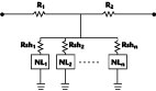
Fig. 1 General T network lossy linearizer topology. |
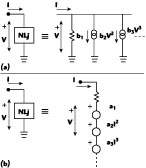
Fig. 2 Power series representation of a one-port nonlinearity; (a) current source model and (b) voltage source models. |
Fig. 3 Representation of a general T network lossy linearizer in terms of equivalent nonlinear current sources. |

Basic Principle of Operation
To begin, the basic T-network is shown in Figure 1 , where NL1 , NL2 ...NLn are one-port nonlinearities. All nonlinearities are assumed to be weak, which enable them to be expressed as a finite power series.8
Now, a one-port nonlinearity NL can be defined8 by the current-voltage relationship

where
k = integer greater than 0
bk = complex in general
The nonlinearity can also be defined by the converse relationship as

A one-port nonlinearity can therefore be represented either by a linear conductance b1 and controlled current sources representing higher degree terms or by a linear resistance a1 and controlled voltage sources, as shown in Figure 2 .
Using the above principle, the generalized lossy nonlinear network can be redrawn as shown in Figure 3 where the current source representation has been used. To a first approximation, its linear equivalent network is shown in Figure 4 , where

is equal to the parallel combination of elements

The fundamental principle of weakly nonlinear networks permits the excitation (I or V) of the one-ports to be calculated using the linear equivalent network. The nonlinear current (or voltage) sources can be computed subsequently. These derived sources, together with the fundamental sources, can be treated as part of a linear network.
Considering the linear approximate model, the linear equivalent network can be designed as a lossy two-port network as appropriate. As an example, it may be a symmetric attenuator with a certain loss and characteristic impedance.
|
|
|
|
|
Fig. 4 Linear equivalent circuit of a T network lossy linearizer. |
Fig. 5 Network generating expansive odd-order nonlinearity. |
Fig. 6 The network's equivalent circuit. |


Some Useful Nonlinearities
Without loss of generality, several examples will illustrate how different circuit topologies can be used to synthesize various types of nonlinearities.
Expansive Odd-order Nonlinearity
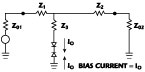
Figure 5 shows a network (without biasing circuit) generating expansive odd-order (mainly third-order for most practical cases) intermodulation products. The network, in general, is asymmetric with image impedances Z01 and Z02 . A special case is a symmetric T-network with characteristic impedance Z0 and nonlinear analysis of the network. A straightforward analysis shown in Appendix A , assuming a weak nonlinearity and a symmetric network, yields the following:
The ratio of signal to two-tone third-harmonic intermodulation IM3 is (in dB)

where the one-port nonlinearity, comprised of pairs of anti-series diodes, is defined by

Pout = output power per tone (W)
The factor F, for a symmetric network (Z1 = Z2 , Z01 = Z02 = Z0 ), is given by

It is also shown in Appendix B that
where
n = number of diode pairs (only one pair is shown)
I0 = bias current through the diodes

q = electronic charge
h = ideality factor of the diodes
K = Boltzmann's constant
T = temperature in degree K
|
|
|
Fig. 7 Examples of networks capable of (even- and odd-order) nonlinearities. |

Even- and Odd-order Nonlinearities
Figure 7 shows examples of networks capable of odd- and even-order nonlinearities, or a combination thereof. Odd-order nonlinearities can either be compressive or expansive, implying a phase shift of p or 0 in the NTF. The sign of even-order NTFs can also be controlled to be p or 0 as desired by selecting the polarity of the diodes.
For the sake of clarity, the biasing circuits have not been shown in the examples. The examples use diodes as the nonlinear element, though other types of devices can also be used.
Design Technique
Any of the network topologies previously discussed can be used to design a linearizer to cancel the nonlinearity of the device to be linearized.
In the following example, an attempt to pre-distort a third-order compressive nonlinearity using the odd-order expansive nonlinearity network is described.
The parameters of interest are third-order output intercept point IP3 , output power, loss in the (equivalent linear) network, bias current through the diodes and the number of diode pairs (a minimum number is preferred to reduce parasitics).
By using Equations 3, 5a and 5b, the IP3 (dBm) can be written as (Appendix A)

Figure 8 illustrates the functional dependence of IP3 on bias current according to Equation 6. An important condition for the successful operation of these types of circuits is that the diodes should not undergo clipping at any instant of time. That is, for clipping not to occur, the peak RF current in the shunt arm cannot exceed the bias current through the nonlinear circuit elements. The above requirement puts a maximum limit on the total available RF power at the output of the circuit. Using the above condition, a lower bound is set on the IP3 (dBm) of the circuit, as described in Appendix A. That is,

where
z = form factor (peak/rms current ratio) of the exciting signal
N = loss of the linear equivalent network in nepers
If the excitation is a multitone signal approaching a Gaussian distribution, z can be taken as 3.
Figure 9 shows the minimum attainable IP3 for the network as a function of loss with the number of diode pairs as a parameter. The output power requirement from the linearizer is assumed to be 0 dBm.
If an IP3 of +21 dBm is required and a loss of more than 7 dB cannot be tolerated, a single diode pair cannot be used to achieve these goals. However, by using two diode pairs, the desired condition is satisfied. This essentially completes the design of the linearizer from a low frequency, or memory-less, standpoint. Therefore, once the loss and the number of diodes are determined, Equation 6 can be used to determine the value of I0 .
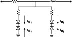
The design has been illustrated with a specific topology, but can be extended to any of the other networks mentioned. There is an infinite number of possible variations, and it is neither possible nor necessary to catalog each and every topology. As an example, one way to satisfy the simultaneous power handling and intercept requirement of the above example is to use the topology of Figure 10 . For a perfectly symmetric network, the two shunt resistances could be combined into one. One has to keep in mind that that if there are multiple shunt arms, Equation 7 must be appropriately modified to include this effect.
|
|
|
|
Fig. 8 IP3 for network of Fig. 5 as a function of bias current with number of diode pairs as parameters. |
Fig. 9 Minimum IP3 attainable for network of Fig. 5 as a function og loss with the number of diode pair as parameter. |
|
|
|
|
Fig. 10 Expansive odd-order nonlinearity modified to handle more power. |
Fig. 11 Generation of I and Q components. |


Use of Various Nonlinear Devices
The examples so far have used diodes as the elements of choice to generate the nonlinearity. Schottky-barrier diodes are the usual choice. However, MESFETs and varactors are also possible candidates.
Figure 11 shows a circuit that generates the in-phase (I) component from Schottky-barrier diodes and the quadrature (Q) component from varactor diodes. Such a configuration is the first step towards the synthesis of a generalized NTF. The arm containing the varactors generates a mixture of I and Q, whereas the one containing the Schottky diodes ideally generates an I component only (resistive arm). The resistive arm current can control the mix of I and Q. The I component generated by the varactor arm is accentuated by the resistive arm. By using anti-parallel diodes instead of anti-series diodes, the I component can be weakened.
Dual Network
Thus far, the basic building block has been a T-network. The same methodology can be applied to p networks as well. The choice of T or p network is often dictated by layout considerations at high frequencies, where it is necessary to reduce the parasitics and approximate the behavior of the circuit to its lumped model as closely as possible.
Broadbanding Techniques
|
|
|
Fig. 12 Equivalent circuit of the expansive odd-order nonlinearity including parasitics. |
Linearizers are often used for broadband applications where the useful frequency range covers several decades. The device to be linearized is often one with a large bandwidth, and has an NTF close to ideal (constant magnitude and phase, 0 or p, over frequency). A typical example is a Mach-Zender modulator used for CATV transmission. To linearize such a device, one needs a nonlinearity close to ideal (memory-less) over the applicable bandwidth.
Though the lossy linearizer is ideally a device with infinite bandwidth, unavoidable parasitics in the circuit elements tend to reduce the useful bandwidth of operation. To achieve the dual goals of intercept point and power handling capacity, one may be forced to use a multiple number of diodes or similar nonlinear elements. The effect of the parasitics becomes more and more severe as the number of such elements goes up. In addition, as the frequency increases, the shunt resistance keeps deviating from its lumped model and keeps adding undesired phase shift. The effect of reactive parasitics manifest itself as a change in the magnitude of the intercept, and a nonlinear phase shift different from 0 or p. The following examples illustrate how the parasitics can be compensated to achieve large bandwidths.
Simple Capacitive Compensation
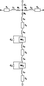
A simplified equivalent circuit, incorporating parasitics, for the expansive odd-order nonlinearity circuit is shown in Figure 12 . The original resistors Z1 , Z2 , Z3 are now represented by ideal lumped resistors (R) in series with inductors (L) and lengths of transmission lines (T). C1 represents the capacitance of the T-junction. NL1 and NL2 represent ideal memory-less nonlinearities, a reasonable model for Schottky diodes forward biased at all instants of time (clipping free operation). Inductances L4 , L5 , L6 , L7 and lengths of transmission lines T4 , T5 , T6 , T7 represent parasitics like lead inductance and bonding pads.
The shunt capacitance C2 , C3 of the diodes, if chosen judiciously, is small and usually produces a large reactance compared to the instantaneous forward resistance of the diodes. Therefore, for reasonable frequencies of operation, forward biased Schottky diodes are closely approximated by memory-less nonlinearities in series with inductors and transmission lines.
The NTF of this circuit is evidently not ideal due to the presence of reactive elements. However, the addition of a compensating capacitor Cc across Z3 and shown in Figure 13 can be used to approximate the NTF to the ideal value within a band of frequencies. Typically, for CATV applications (50 to 750 MHz), it is possible to find a value of the compensating capacitor that maintains the magnitude of the NTF within ±0.25 dB and phase within ±5°.
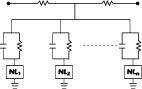
The capacitor tends to bypass the high frequency components of the current flowing through Z3 and make them reach the nonlinearity faster than it would have reached otherwise, and tends to compensate the finite delay in the transmission lines T3 , T4 , T5 and inductors L3 , L4 , L5 , L6 , L7 . Figure 14 shows how the capacitive compensation can be applied to a lossy linearizer having multiple arms.
To meet the power handling requirements, one is often to forced to use multiple diodes or diode pairs, adding to parasitics. To avoid this situation, a circuit with two diode pairs in two arms can be used instead of one diode pair in a single arm. However, multiple shunt arms tend to increase the parasitic capacitance C1. To keep the number of shunt arms reasonable, cascaded linearizers could be used.
|
|
|
|
Fig. 13 Capacitive compensation to reduce effect of parasitics. |
Fig. 14 Capacitive compensation for linearizer with multiple shunt arms. |

Application Example
A typical application of the use of this class of linearizers to pre-distort a electroabsorption modulated laser (EML) is shown, although the application is not limited to EML devices only. The modulator was pre-distorted over the 50 to 750 MHz band to carry multiple carriers over this band.
Prior art10 using current modulation suffers from reduced bandwidth. Yu, et al.,11 uses a companion EML device, and is therefore cost-prohibitive. Impressive results have been reported by Wilson, et al.,12 using a feed-forward technique, which tends to be rather elaborate.
A circuit generating simultaneous even- and odd-order nonlinearities was constructed on standard FR-4 board with surface-mount type 0603 components and used to pre-distort an EML device operating at 1558.98 nm. The excitation consisted of eight CW carriers (to simulate the narrow-cast signals) each with an optical modulation index (OMI) of 7.4 percent, resulting in a peak composite OMI of approximately 45 percent. The carriers were located within the 50 to 750 MHz band and the worst case composite second-order (CSO) and composite triple beat (CTB) was observed. The worst case CSO, occurring at 721 MHz, was improved from -41 dBc to -50 dBc, and the worst case CTB, occurring at 55 MHz, was improved from -42 dBc to -50 dBc.
Conclusion
A general technique for synthesis of broadband linearizers has been presented. The resulting circuitry is simple to implement and tune. The technique has been successfully applied to linearize an electroabsorption modulated laser to carry narrow-cast signals for CATV networks.
References
1. M. Nazarathy, et al., (US Patent US5424680), "Predistorter for High Frequency Optical Communcations Devices," 1995.
2. J.S. Bitler, (US Patent 6,122,085), "Lightwave Transmission Techniques," 2000.
3. C.Y. Kuo, (US Patent US5418637), "Cascaded Distortion Compensation for Analog Optical Systems," 1995.
4. M. Nazarathy, et al., (US Patent US5161044), "Optical Transmitters Linearized by Means of Parametric Feedback," 1992.
5. R. Pidgeon, (US Patent US5850305), "Adaptive Predistortion Control for Optical External Modulation," 1998.
6. H.A. Blauvelt, et al., (US Patent US5798854), "In-line Predistorter for Linearization of Electronic and Optical Signals," 1998.
7. R. Pidgeon, (US Patent 6204718), "Method and Apparatus for Generating Second-order Predistortion without Third-order Distortion," 2001.
8. S. Maas, Nonlinear Microwave Circuits, Artech House, 1988.
9. S. Mukherjee, "Vector Measurement of Nonlinear Transfer Function," IEEE Transactions on Instrumentation & Measurement , Vol. 43, No. 4, August 1994.
10. G.C. Wilson, et al., "Integrated Electroabsorption Modulator/DBR Laser Linearized by RF Current Modulation," IEEE Photonic Technology Letters , Vol. 7, No. 10, October 1995.
11. J.Yu, et al., "Linearization of 1.55 mm Electroabsorption Modulated Laser by Distortion Emulation and Reversal for 77-channel CATV Transmission," IEEE Photonic Technology Letters , Vol. 10, No. 3, March 1998.
12. G.C. Wilson, et al., "Pre-distortion of Electroabsorption Modulators for Analog CATV Systems at 1.55 mm," IEEE J. Lightwave Technology , Vol. 15, No. 9, September 1997.
Somnath Mukherjee has more than 15 years of extensive engineering experience, mostly as project leader in the development of systems and subsystems for Hybrid Fiber Coax (HFC) networks. He has also worked in the areas of high frequency measurement and wireless communication. As the key technical leader at Silicon Valley Communications, he led the development team that resulted in the acquisition of the company by C-COR.net. Earlier at Harmonic Inc. he made significant contributions to develop the core technical competence of the company. He has a master's degree in technology from the Institute of Radio Physics and Electronics, Calcutta, India, his MSEE from Syracuse University and his PhD in engineering from the University of Kansas. He has published several journal and conference articles, and is the holder of two US patents. Dr. Mukherjee received the best paper award at the IEEE-MTT (ARFTG) conference in 1991. His areas of interest include RF-optics interaction, nonlinear RF circuits, high frequency measurement, etc.
Mridul K. Pal received his BSc in physics, and his B Tech and M Tech degrees in radio physics and electronics from the University of Calcutta, India, in 1988, 1991 and 1993, respectively. Currently he works as a senior RF development engineer at C-COR.net.
Ralph Inducta received his BS degree in electrical engineering from San Jose State University in 2000. He is currently pursuing his MS degree from the same school. In 2000 he joined C-COR.net under Dr. Mukherjee's R&D team in Santa Clara, CA. He is now a RF/Fiber-optic development engineer with C-COR.net research and development group. Mr. Inducta is a member of Tau Beta Phi and the IEEE Lasers & Electro-optics Society (LEOS).