
Technical Feature
Fractional-N Synthesizers
David Owen
IFR Systems Inc.
Wichita, KS
|
|
|
Fig. 1 A basic fractional-N system with no jitter correction based on a single accumulator. |

Fractional-N synthesizers have been used for many years to improve the performance of indirect frequency synthesizers. A simple indirect synthesizer consists of a phase-locked loop (PLL) in conjunction with frequency dividers, but the frequency resolution of such a synthesizer is limited by the phase detector rate - if a 1 kHz phase detector rate is used, then the resolution will also be 1 kHz. However, many applications demand much finer frequency control, and for this reason, a technique known as fractional-N synthesis was developed.
Figure 1 shows its principle of operation. The division ratio of the divider is made to have a fractional component by changing the division ratio of the divider periodically, so an average value contains a fractional element. If, for instance, a fractional value of 0.1 is required, then the division ratio is changed by 1 every tenth cycle. If a fractional value of 0.01 is required then the division ratio is changed by 1 on every one-hundredth cycle. This offers much finer frequency control than integer-based systems.
An accumulator whose digital output is incremented for each cycle of the divider by the fractional frequency instruction is a convenient method of controlling the division ratio because the carryout occurs when the divider ratio needs changing.
In the previous example, if the accumulator has a 0.1 fractional instruction added to its output for each clock cycle then the accumulator will be full and overflow every tenth cycle. In a similar way, if the fractional instruction is 0.01, the accumulator will overflow every 100 cycles.
|
|
|
Fig. 2 Block diagram of an early fractional-N synthesizer using analog correction. |

There is a price to be paid for the improvement in the frequency resolution that these systems provide. The manipulation of the divider ratio generates phase perturbations, and hence spurious signals, which must be eliminated in a useful synthesizer design. The nature of the phase perturbations is predictable and can be canceled using an analog correction system. Solutions that use various techniques to improve the performance of PLLs based on the fractional-N system have been patented.1-5
A fractional-N synthesizer system with analog correction was used in the design of a 10 kHz to 1 GHz signal generator to provide 10 Hz resolution based on a phase detector rate of 40 kHz. Its block diagram is shown in Figure 2 . An accumulator that changes the division ratio by 1 each time the accumulator overflows controls the divider.
The content of the accumulator represents the residual phase error in the PLL and, by routing this signal to a D-to-A converter and applying the analog signal to a phase modulator within the PLL, the residual errors can, in principle, be eliminated, as shown in Figure 3 .
With a small fractional frequency instruction at the input to the fractional-N system the output of the accumulator increases in its digital value on each cycle of the phase detector clock. The residual phase error in the PLL also accumulates in the same way. When the accumulator overflows (that is, its content becomes greater than the capacity of the accumulator), the divider division ratio is changed by one for one cycle of the phase detector. Changing the division ratio by one for one cycle of the phase detector effectively absorbs one cycle of the VCO frequency, and hence introduces a 360° phase shift. The digital-to-analog (D-A) converter produces an analog representation of the PLL accumulated phase error and is used to phase modulate the PLL to cancel the analog error.
|
|
|
Fig. 3 Analog correction of the phase jitter in a fractional-N system. |

The amplitude of the correction system must also be scaled as the average output frequency (and therefore the average division ratio) in the PLL changes. This arises because the phase modulator acts at a constant frequency (the phase detector rate) and a phase change (or time change) at the detector has a different phase impact on the VCO according to the division ratio of the divider.
However, there is a limit to the accuracy of the cancellation that can be achieved, and obtaining cancellation of better than 1 percent can be troublesome. In addition, the use of analog components to correct for the error results in a design that requires careful setting up and can drift with time.
The need to apply analog correction to such synthesis schemes also has the effect of restricting the phase detector rate that can be used. This stems from the need to run the correction circuitry conservatively in order to maintain good accuracy and linearity, and from the need to avoid the injection of wideband noise from the correction system.
For optimum performance, in terms of speed and noise, a PLL should be operated at the highest practical phase detector rate to minimize divider ratios and give the highest margin between the loop bandwidth and phase detector frequency. It is clear that there are significant design compromises needed when designing PLLs of this type.
King6 described an improved version of a fractional-N system. This configuration used two accumulators, but still required analog correction in order to minimize spurious responses. An ideal fractional-N system would not require any analog components in order to cancel these residual phase errors. Intuition at the time suggested that this was not a practical possibility, but an all-digital solution was found. The all-digital solution results in a PLL performance that is virtually indistinguishable from the non-fractional loop operating at the same phase detector rate, and is capable of operating at much higher phase detector rates than those that relied on analog correction techniques.
Fractional-N System with Digital Correction
|
|
|
Fig. 4 Fractional-N system using digital correction. |
The digital fractional-N system is based on the principle of noise shaping proposed by Wells.7 Rather than trying to cancel the phase errors, this system modifies their pattern so as to minimize low frequency spectral content. The technique actively reduces the generation of these low frequency signals and exchanges them for increased levels of higher frequency signals. (A simple implementation of this system is shown in Figure 4 .)
Within the context of the PLL this is a highly satisfactory arrangement because the loop itself acts as a low pass filter. Additional low pass filtering can then be included within the loop filter to prevent any of the modified perturbations from significantly modulating the voltage-controlled oscillator.
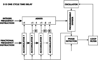
In the example, the single accumulator of the earliest forms of the fractional-N synthesizer is replaced with three or more accumulators, the output of each connected to the input of the next. The overflow from each of the accumulators manipulates the division ratio of the divider.
Effect of Accumulator Overflows
The first accumulator overflow acts in the same way as the accumulator in the simplest fractional-N systems; it changes the division ratio divider from N to N+ 1 for one cycle when the accumulator overflows. The remaining output from the first accumulator symbolizes the phase error that would result if no other correction were applied.
The second accumulator digitally integrates the output of the first accumulator and subsequent accumulators repeat this process. The question then arises as to how to manipulate the division ratio of the divider in order to reduce the low frequency phase jitter that it produces on its output. The solution is that the overflow from the second accumulator needs to manipulate the division ratio by the differential of the effect of the first accumulator. In a similar way the output from the third accumulator manipulates the division ratio by the differential of the effect that an overflow output from the second accumulator causes, and so forth.
The first accumulator produces a change of division ratio that changes from N to N+1 and then back to N. The second accumulator carry overflow is required to generate a sequence that changes from N to N+1 and then to N-1 and then to N, when an overflow is initiated. In a similar way the third accumulator overflow changes the division ratio from N to N+1 then to N-2, then N+1 and then returns to N. A fourth accumulator would use a sequence N+1, N-3, N+3 and N-1.
|
|
|
Fig. 5 Pattern of division ratio changes caused by accumulator overflows shown as a Pascal triangle. |

The sequences that are generated correspond to a Pascal triangle, as shown in Figure 5 , but with the overall sum of each row weighted to be zero, with the exception of the first, which is required to correct the overall division ratio of the divider in order to obtain the required fractional frequency. Because the second and subsequent rows of the Pascal triangles introduce an average divider change of 0, these accumulator overflows have no long-term effect on the division ratio of the divider. However, they do serve to remove low frequency components from the divider's output spectrum and to transfer the energy to higher frequencies where they can be successfully filtered by the PLL.
The accumulator overflows can all be routed via a cascade of single-clock-period delay networks (implemented by D-type flip-flops) and an adder with weighted inputs so that they generate the required division ratio changes.
Alternative Circuit Implementation
|
|
|
Fig. 6 A different circuit implementation of the fractional-N system. |

The original implementation was drawn in the manner previously described. However, the same effect can be obtained from the redrawn version shown in Figure 6 .
The accumulators can be considered to be digital integrators. The weighting functions generated by the overflow are generated by differentiating the effect of the previous accumulator's overflow.
An overflow is differentiated by turning an accumulator overflow into an N+1, N-1 sequence. This sequence is generated by initially passing the overflow directly to an adder, and then passing an inverted version one-clock cycle later to the same adder. If the resulting signal from each overflow is tracked through the chain of summers, delay (D) and inverter (I) circuits, the same Pascal's triangle sequence as that disclosed in Wells is built up. Replacing the differentiating function (N converted to N+1, N-1) with an alternative function leads to sequences other than Pascal's triangle with broadly similar levels of performance; however, Pascal's triangle solution is the simplest and optimum solution.
Understanding the Improvement
|
|
|
Fig. 7 Pictorial view of the effect of the accumulator overflows on residual phase error in the PLL. |

A pictorial representation of how the phase jitter is reduced is shown in Figure 7 . In this diagram the fractional component of the frequency instruction is relatively high, but it does give an indication of the sort of mechanisms at work. The target phase is a representation of the required phase of the VCO if there were no phase jitter present. In the first plot, using one accumulator (the simplest form of fractional-N), the division ratio of the divider is changed from N to N+1. This introduces an abrupt 360° change in phase that corrects the accumulated phase error of the VCO. The residual phase jitter is clearly a ramp with the residual phase error being equal to the remainder output of the first accumulator, the same as was disclosed for simple fractional-N systems.
The second plot shows the effect of introducing a second accumulator. The second accumulator overflows much more often than the first and a phase perturbation is introduced much earlier.
When the accumulator overflows, division ratios of N+1, N-1 on successive clock cycles are introduced. As can be seen from the plot, the area under the positive phase transient is approximately equal to the area below the target phase, so after this overflow the average area in accumulated phase is now much smaller than it would have been. This sequence of events is repeated through the fractional cycle. As the content of the first accumulator increases (that is, getting closer to an overflow) the second accumulator overflows more often. If one imagines what the plot would look like after passing through a low pass filter the error is clearly less than that shown in the first plot.
The removal of the low frequency content in the output from the phase detector is not perfect, however, and must be further reduced in a useful synthesizer design. The third accumulator overflows more frequently than the second accumulator, and the third plot shows the effect of this third accumulator. The first N+1, N-2, N+1 sequence starts at an earlier point in time. In fact, the accumulator overflows so often that overflows tend to be superimposed on top of one other. The phase correction starts much earlier in the cycle and occurs much more often. Greater division ratio changes occur, but if the results are passed through the PLL filter, the end result is a signal whose low frequency content is much lower, and because most of the high frequency content can be removed by the PLL filter, the overall performance of the loop is much improved.
|
|
|
Fig. 8 Noise shaping introduced by the fractional-N system. |

The impact of this process can be simulated and plotted. The impact of the noise and jitter in fractional-N systems averaged over a large number of possible fractional division ratios is a flat (white) noise signal. This is not surprising since the peak-to-peak jitter is always 360° - the first accumulator limits the peak error. A similar analysis can be performed on the three accumulators using commercially available mathematical tools running on a PC. (When the original simulations were done on fractional-N, it took up to one hour of CPU time on a main frame computer to do a simulation representing less than one second of operation of the system.) The results of such a simulation are shown in Figure 8 .
Instead of being flat, the noise profile is frequency shaped. The low frequency noise is much lower than the 0 dB reference line. The higher frequency noise is actually higher than for an uncorrected system (as usual, a gain is never achieved without a penalty). The slope of the noise is dependent on the number of accumulators Ñ the more accumulators the steeper the slope and the more the high frequency noise is lifted. It can be shown that the accumulators can be added ad infinitum to shape the resulting phase noise progressively and give less and less low frequency content. However, most systems require only three accumulators before the resulting spurious signals are virtually eliminated from a practical design.
There are good reasons for not adding more accumulators than are required because, as the number of accumulators increase, the division ratio excursions and high frequency signal content increase. This results in greater excursions in peak phase error at the input to the phase detector, and nonlinearity in the phase detector can cause high frequency products to be intermodulated down to lower frequencies. For this reason, the phase detectors used in the implementation of this fractional-N system use a highly linear, digitally-based phase detector that avoids the dead zones and nonlinearities associated with the more conventional dual D-type phase detectors. However, continued addition of accumulators creates the need for an ever-widening range of division ratios and that causes problems with the design of programmable dividers. The ultimate limit, of course, is set by the need to keep all the ratios positive. The design compromise is essentially one of using enough accumulators, but not more than is required since it would increase the division ratio required in the PLL and impose greater levels of performance on the phase detector.
Comparing Performance
The performance of a particular design can be assessed by operating the fractional-N synthesizer system with the fractional component of the frequency instructions set to zero. If the content of the first and subsequent accumulators are all set to zero, then, with no fractional instruction into the first accumulator, the synthesizer will behave as a conventional integer PLL. If, however, a random number is inserted into the output of the first accumulator then all of the subsequent accumulators will change and generate accumulator overflows. This will result in the synthesizer generating sequences of division ratio changes that have no net effect on the division ratio; however, if the design of the PLL is imperfect it will degrade the performance of the fractional-N synthesizer system because of nonlinear behavior. With careful design, it is possible to make a fractional-N synthesizer based on this technique, whose performance is indistinguishable operating in the integer mode from its operation in the fractional mode.
DC-Coupled FM
|
|
|
Fig. 9 DC-coupled FM circuits added to the fractional-N system using one-bit A-D converter technology. |

For synthesizer schemes used in signal generators there is a requirement that the system should enable the use of frequency modulation, and many applications, such as frequency shift keying (FSK) systems used for paging, require that the frequency modulation allows DC control of the synthesizer's output frequency. Traditionally this has been a difficult technical problem, often solved by using complex analog solutions to the implementation, which give marginal performance.
The IFR fractional-N system lends itself to a DC-coupled FM system8 based on the use of a one-bit A-D converter, as shown in Figure 9 . As with the fractional-N system this A-D converter is substantially over-sampled so that it can be noise-shaped, in much the same way CD quality A-D converters now operate. The system is extremely effective when used with the new fractional-N system because it virtually eliminates carrier-frequency error in the DC-coupled FM mode.
The FM signal is applied directly to the VCO to produce FM outside the PLL bandwidth. Inside the PLL bandwidth, the fractional-N divider is used to manipulate the frequency setting of the synthesizer in sympathy with the required FM signal. The fractional-N divider is controlled by applying the analog signal to a third-order feedback system deployed around a one-bit D-A converter - it simply decides whether the error signal is greater than or less than 0 V for each clock cycle of the phase detector.
The analog feedback is stabilized by making two of the three integrators have unity again above a break frequency so that the loop is stable. The gain of the feedback system increases with lower modulation frequencies, so the noise of the signal sent to the divider is much lower at low offsets than at high offset frequencies. To understand how the system operates it is not necessary to understand the detail of the pattern of logic 1s and 0s that the digital output produces. Instead, consider the system to be a simple feedback circuit with a digitizer (the one-bit converter) adding noise (quantization noise). The feedback system automatically forces the pattern of data to reduce the noise at low frequencies since the gain of the feedback increases with lower frequency. Just like the fractional-N system itself, the DC FM system is noise shaped and takes advantage of the fact the PLL rejects the higher frequency components introduced. The magnitude of the frequency (divider) changes introduced by the 1s and 0s from the DC FM system determines its sensitivity. The result is that the DC FM system is exceptionally well behaved. The DC error in the system is simply related to the DC errors in the analog operational amplifiers used - there is no reliance on RF components in oscillators being stable with time or temperature.
|
|
|
Fig. 10 FM modulation response diagram. |

The use of two-port modulation (modifying the oscillator and the divider with a FM signal) requires that the two paths are calibrated so they have the same gain and their phases are matched. As Figure 10 shows, at low modulation frequencies the FM is generated by the digital DC FM system while higher frequencies are provided by analog modulation of the VCO. If there is any mismatch in the two paths, a frequency response error is observed around the PLL bandwidth. A separate automatic system that achieved this with a coherent detector arrangement to match the gain of the DC FM path and the VCO path is described in reference 9. The DC FM system based on a one-bit converter also has the great advantage of introducing very little time delay into the DC path, making it relatively easy to match the DC path and the analog (VCO) path. What remaining errors in phase are present can be matched by using digital prediction systems.
Conclusion
Fractional-N systems have been used in commercial signal generators since 1989. Covering ranges of 1.35 GHz and 2.7 GHz, these first generators offered 0.1 Hz frequency resolution and a DC-coupled FM performance, which is still state-of-the-art.
The system has been used in microwave synthesizers for microwave test sets. The inherent speed advantages and simple design have resulted in low cost, agile, synthesized sources, which can allow fast scalar and distance-to-fault measurements in future microwave systems.
References
1. N.B. Braymer, "Frequency Synthesizer," US Patent 3555446, 12 January 1971.
2. G.C. Gillette, "Frequency Synthesizer," US Patent 3582810, 1 June 1971.
3. M.J. Underwood, "Frequency Synthesizer," UK Patent 1447418, filed 29 March 1974, published 25 August 1976.
4. R.G. Cox, "Frequency Synthesizer," US Patent 3976945, 24 August 1976.
5. C.A. Kingsford-Smith, "Device for Synthesizing Frequencies Which are Rational Multiples of a Fundamental Frequency," US Patent 3928813, 23 December 1973.
6. N.J.R. King, "Phase-locked Loop Variable Frequency Generator," US Patent 4204174, 20 May 1980.
7. J.N. Wells, "Frequency Synthesizers," European Patent EP 125790, filed 11 April 1984, published 21 November 1984.
8. N.E. Thomas, European Patent EP 322139, filed 8 December 1988, published 28 June 1989.
9. D.P. Owen and J.N. Wells, "US 5079522 Variable Frequency Signal Generator," priority 20 October 1989.
Copies of some of these patents can be obtained from the Patent Office Web sites.
David Owen joined Marconi Instruments as a student in 1968, graduating with a BSc in 1972 in electrical and electronic engineering from Hatfield Poly (University of Herts). He has been involved extensively as the project leader for the 2018 series, project leader and then engineering manager for the 2030 series, then becoming product manager for signal sources and analyzers. Mr. Owen next worked in a strategic marketing role for five years before becoming the signal sources business manager in 2000.