
Technical Feature
An Automatic Macro Program for Radio Frequency MOSFET Characteristics Analysis
The parameter extraction language (PEL) in Agilent IC-CAP software is used to develop an automatic macro program for the analysis of the characteristics of RF MOSFETs. By using this powerful macro program, the time spent on the measurement of the MOSFET characteristics and the related analysis is effectively reduced. This macro program permits a fast and accurate method to obtain the DC and RF characteristics of MOSFETs with different device geometries and operating conditions. It is also suitable for high volume measurements and analyses of MOSFETs, and provides a solid foundation for RF circuit design.
C.Y. Su and S.J. Chang
National Cheng Kung University
Department of Electrical Engineering
Tainan, Taiwan, R.O.C. L.P.
Chen and Y.P. Ho
Giga Solution Technology Co.
Hsinchu, Taiwan, R.O.C.
G.W. Huang, D.C. Lin, B.M. Tseng, H.Y. Lee, J.F. Kuan and Y.M. Deng
National Nano Device Laboratories
Hsinchu, Taiwan, R.O.C.
K.A. Wen and C.Y. Chang
National Chiao Tung University
Department of Electronics Engineering and Institute of Electronics
Hsinchu, Taiwan, R.O.C.
With the dramatic advances in silicon very large scale integration (VLSI) technology, on-chip silicon radio frequency integrated circuits (RFIC) have recently emerged as attractive candidates for use in rapidly growing wireless communications applications.1-4 These applications, based on Si technology, can profit by the increase in integration density of RF, baseband and digital signal processing (DSP) modules. The systems implemented with high integrity silicon technologies also show improved reliability and reduced power consumption as compared to systems that are based on compound materials.
Unfortunately, semi-conducting silicon substrates introduce substantial substrate losses which degrade significantly the performance of Si-based devices at microwave frequencies.5-9 Therefore, it is not easy to predict or model the behavior of Si-based active or passive devices such as MOSFETs and inductors at high frequencies.8,9 Accurate measurements of S-parameter and de-embedding using dummy devices are necessary.10,11 The procedures for obtaining accurate device characteristics often take a long time. In this article, an automatic macro program for the analysis of the characteristics of RF MOSFETs is described that overcomes this issue. The macro program integrates the procedures for measurement, de-embedding and relative analysis to obtain the DC and RF characteristics of MOSFETs with different device geometry and operation conditions, rapidly and accurately. The characteristic parameters of MOSFETs obtained play an important role in modeling the behavior of Si RF MOSFETs for the design of on-chip silicon RFICs.
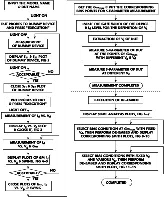
Fig. 1 Flow chart of programmed measurement and analysis macro.
The Macro Program
Measurement Macro
|
|
|
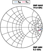
Fig. 2 S11 and S22 curves of dummy pad. |
The two-port S-parameters are measured with an Agilent 8510 network analyzer and Cascade Microtech coplanar GSG probes. The PEL in Agilent IC-CAP software is utilized to develop the measurement and characteristics analysis macro. Here the parasitic effects of probe pads are de-embedded with an "open" dummy device. The measurement macro is functionally divided into three parts - measurement of the dummy device, DC performance and S-parameter characteristics.
Figure 1 shows the flow chart of the macro program. The algorithms used are described below. The macro program begins by entering the name for the device under test (DUT). The light source projected onto the DUT is turned on automatically. Then the GSG probes are set onto the dummy device and "Execution" as requested by the dialog box is clicked. The macro program automatically turns off the light source and begins to measure the characteristics of the dummy device. Because the measured S-parameters of the MOSFET consist of the combined characteristics of the intrinsic MOSFET and dummy pads used for probing, the parasitic effect of the dummy pads must be subtracted through a correction procedure10 to obtain the intrinsic performance of the MOSFET. When the measurements of the dummy device are completed, the system displays the measured S11 and S22 curves for the dummy device, as shown in Figure 2 .
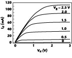
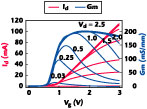
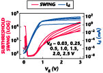
If the measured results for the dummy device are acceptable, the GSG probes are set on the DUT and the "Execution" command will continue the measurement of the DC characteristics of the MOSFET and display the corresponding results as shown in Figures 3, 4 and 5 . The DC measurements also provide some DC characteristics of the MOSFET, such as transconductance (Gm), output resistance (Rout ), subthreshold swing and drain induced barrier lowering (DIBL), and gives the required information for modeling and predicting the DC performance of the MOSFETs. If the measured results are acceptable, the macro will automatically evaluate the corresponding bias conditions at which the maximum Gm (Gmmax ) occurs for the S-parameter measurements that follow.
|
|
|
|
|
Fig. 3 The curves of Id vs. Vd . |
Fig. 4 Dependence of Id and Gm on Vg bias. |
Fig. 5 Dependence of subthreshold swing and Id on Vg bias. |
The S-parameter measurements mainly consist of two parts. The first one measures the S-parameters at which the Gmmax occurs under different Vd bias, and the other one measures the S-parameters at any bias conditions desired. Many high frequency characteristics of a MOSFET have a strong dependence on its transconductance. The cut-off frequency (Ft ) and the maximum oscillation frequency (Fmax ) can be approximately given as12
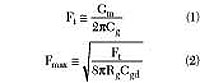
where
Cg = Cgs + Cgd
Cgs = gate-source capacitance
Cgd = gate-drain capacitance
Rg = gate resistance
These two equations imply that Ft and Fmax are the largest at Gmmax . Therefore, the S-parameter measurements at the bias point corresponding to Gmmax may give an indication of the performance of MOSFETs under different Vd bias. Before measuring the S-parameters of the DUT at Gmmax , the gate width of the device and the drain current level for the threshold voltage (Vt ) determination must be defined to evaluate the threshold voltage of the MOSFET as described in the program flow chart. After finishing the S-parameter measurements at Gmmax , the macro program will automatically continue to measure the AC characteristics of the DUT at the desired bias conditions. As is well known, the operating point of MOSFETs used in circuit designs does not always coincide with Gmmax , thus, the S-parameter characteristics of the MOSFETs at other bias conditions must be measured. Now the S-parameter characteristics of the dummy device, and the measurements of DC and RF characteristics of the MOSFET have been concluded. The DC and RF characteristics of MOSFETs can be easily and smoothly obtained by following the instructions given in the dialog box of the macro program.
|
|
|
|
Fig. 6 Dependence of the magnitude of h21 on Vg with different Vd bias at 1.2 GHz. |
Fig. 7 Dependence of Ft on Vg bias before and after de-embedding. |
De-embedding and Analysis Macro
When operating at high frequencies, some energy is transmitted through the lossy silicon substrate. This degrades the performance of the MOSFETs and the parasitic effects of dummy pads must be taken into account. Better MOSFET frequency responses are generally achieved by scaling down the device dimensions, such as smaller gate length, which results in a reduction of the transistor intrinsic parasitics, such as a smaller gate parasitic capacitance. However, for high frequency measurement, the probe pad and interconnect configurations are not significantly scaled as well as the device's dimension. Therefore, the parasitics of the probe pads have a large influence on the measured characteristics of the MOSFETs. The parasitic effect of dummy pads must be subtracted out by a correction procedure,10 that is, de-embedding, to obtain the intrinsic performance of the MOSFET.
|
|
|
Fig. 8 Dependence of the magnitude of h21 on Vg with different Vd bias at 1.2 GHz. |
Using the Agilent 8510C vector analyzer, and calibration standards (ISS) and probes from Cascade Microtech, moving the reference planes to the probe tips gives enough accuracy to measure the high frequency characteristics of devices with large dimensions. However, additional de-embedding structures are needed for smaller devices. For example, the most popular structure to remove the parasitic capacitance of dummy pads is an "open" dummy. "Short" or "through" dummy structures are also optionally used to further remove the parasitic resistance or inductance of dummy pads.
|
|
|
|
|
Fig. 9 Dependence of short-circuit current gain, and maximum stable and maximum available gains on frequency with Vd =2.5 V at Gmmax . |
Fig. 10 Dependence of S21 on frequency with Vd =2.5 at Gmmax. |
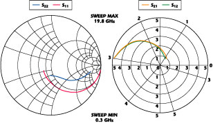
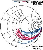
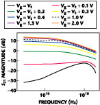
Fig. 11 MOSFET S11 and S22 curves with Vd =2.5 V and Vg = Vt Vt + 0.1, Vt +0.2, Vt +0.3, Vt +0.4, Vt +0.5, 1.0 1.5, 2.0 and 2.5V. |
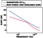
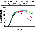
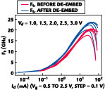
After the measurement of MOSFETs are finished, the macro program will de-embed the parasitic effects after measuring the S-parameters of the "open" dummy device and display the de-embedded results. For example, Figure 6 shows the dependence of the short-circuit current gain (h21 ) on Vg bias at 1.2 GHz with different Vd bias. Similar curves can be obtained for different frequency points as desired. Figure 7 shows the dependence of Ft on drain current (by sweeping the Vg bias) for different Vd bias before and after de-embedding. It demonstrates the difference with or without de-embedding. Figures 8, 9 and 10 show the plots of S11 and S22 , and the dependence of short-circuit current gain, maximum stable/ available gain and S21 on frequency with the DUT biased at Gmmax with a fixed Vd = 2.5 V. Figures 11, 12, 13, 14 and 15 show the same characteristics for the DUT biased at various Vg with Vd = 2.5 V. RF circuit designers can pick the most appropriate bias point to realize on-chip RFICs by scrutinizing the MOSFET characteristics for different bias conditions. Through the execution of the macro program, which integrates the measurement, de-embedding and relative analysis procedures, important characteristics of a MOSFET can be obtained fast and accurately. The time consumption for the measurement of RF MOSFETs and related characteristics analysis can be reduced effectively. The obtained accurate characteristics of the MOSFETs give a basis to help model the behavior of Si RF MOSFETs for on-chip communication circuit applications.
|
|
|
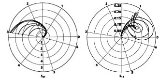
Fig. 12 MOSFET S21 and S12 curves with Vg =2.5V and Vg =Vt Vt +0.2, Vt +0.3, Vt +0.4, Vt +0.5, 1.0, 1.5, 2.0 and 2.5 V. |
Conclusion
Using the powerful macro program that integrates measurement, de-embedding and relative analysis procedures, important characteristics of MOSFETs, such as DC performance, short-circuit current gain and cut-off frequency, can be obtained fast and smoothly. The macro program not only makes it fast and accurate to obtain the DC and RF characteristics of MOSFETs with different device geometry and operating conditions, it also plays an important role in helping to model the behavior of Si RF MOSFETs. The macro program can handle high volume measurement and characteristics analysis of MOSFETs, and help in realizing on-chip silicon circuits for wireless communication applications.
|
|
|
|
|
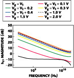
Fig. 13 Dependence of h21 magnitude on frequency with Vd =2.5 V various Vg biases. |
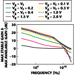
Fig. 14 Dependence of maximum stable and maximum available gains on frequency with Vd =2.5 V and various Vg biases. |
Fig. 15 Dependence of S21 magnitude on frequency with Vd = 2.5 V and various Vg biases. |
References
1. P.R. Gray and R.G. Meyer, "Future Directions in Silicon IC's for RF Personal Communications," Proceedings of the IEEE Custom Integrated Circuits Conference , May 1995, pp. 83-90.
2. L.E. Larson, "Integrated Circuit Technology Options for RFIC's - Present Status and Future Directions," IEEE Journal of Solid-State Circuits , Vol. 33, March 1998, pp. 387-399.
3. J.H. Mikkelsen and T.E. Kolding, "RF CMOS Circuits Target IMT-2000 Applications," Microwaves & RF , July 1998, pp. 99-107.
4. D.K. Shaeffer and T.H. Lee, "A 1.5 V, 1.5 GHz CMOS Low Noise Amplifier," IEEE Journal of Solid-State Circuits , Vol. 32, May 1997, pp. 745-759.
5. N. Camilleri, J. Kirchgessner, J. Costa, D. Ngo and D. Lovelace, "Bonding Pad Models for Silicon VLSI Technologies and Their Effects on the Noise Figures of RF NPNs," IEEE Microwave and Millimeter-wave Monolithic Circuits Symposium Digest , 1994, pp. 225-228.
6. J.R. Long and M.A. Copeland, "The Modeling, Characterization and Design of Monolithic Inductors for Silicon RF IC's," IEEE Journal of Solid-State Circuits , Vol. 32, March 1997, pp. 357-369.
7. M. Park, S. Lee, C.S. Kim, H.K. Yu, J.G. Koo and K.S. Nam, "The Detailed Analysis of High Q CMOS-compatible Microwave Spiral Inductors in Silicon Technology," IEEE Transactions on Electron Devices , Vol. 45, September 1998, pp. 1953-1959.
8. N.M. Nguyen and R.G. Meyer, "Si IC-compatible Inductors and LC Passive Filters," IEEE Journal of Solid-State Circuits , Vol. 25, August 1990, pp. 1028-1031.
9. J.N. Burghartz, M. Soyuer and K.A. Jenkins, "Microwave Inductors and Capacitors in Standard Multilevel Interconnect Silicon Technology," IEEE Transactions on Microwave Theory and Techniques , Vol. 44, January 1996, pp. 100-104.
10. H. Cho and D.E. Burk, "A Three-step Method for the De-embedding of High Frequency S-parameter Measurements," IEEE Transactions on Electron Devices , Vol. 38, June 1991, pp. 1371-1375.
11. C.H. Kim, C.S. Kim, H.K. Yu and K.S. Nam, "An Isolated-open Pattern to De-embed Pad Parasitics," IEEE Microwave and Guided Wave Letters , Vol. 8, February 1998, pp. 96-98.
12. T. Manku, "Microwave CMOS - Device Physics and Design," IEEE Journal of Solid-State Circuits , Vol. 34, March 1999, pp. 277-285.