
TECHNICAL FEATURE
SiGe Power Amplifier ICs with SWR Protection for Handset Applications
In recent years there has been enormous growth in the wireless communications industry, placing a tremendous demand on the semiconductor industry for integrated circuits. For example, DataQuest projects the total market for semiconductors in wireless handsets alone to grow to approximately $35B by the year 2004. As wireless communication standards evolve to the next generation, the largest growth in services is projected in the area of integrated voice and data networks, which provide Internet protocol-based connectivity.
As a result of the increase in bandwidth-intensive wireless services, new demands will be placed on the semiconductors that support RF subsystems in wireless portable devices. Specifically, RF semiconductor components will require higher operating speeds, higher linearity (particularly at reduced supply voltages), better efficiency and higher levels of integration. The availability of multifunction, mixed-signal ICs with considerable RF system content will become even more critical. SiGe bipolar complementary metal-oxide semiconductor (BiCMOS) technology has recently received a lot of attention as a suitable technology for RF/analog and mixed-signal applications.1 However, until now, SiGe has not been considered a suitable technology for power amplifier (PA) applications, primarily due to the lower breakdown voltages of SiGe NPN devices compared to their GaAs HBT counterparts.
This article describes how SiGe technology has been used to develop a family of five PA ICs that address all major protocols for wireless handsets as they evolve from the present to 3G requirements. The evolution to these newer protocols will occur alongside the present ones, resulting in continued demand for a wide variety of power amplifier types. The roadmap in Figure 1 shows how the family of SiGe power amplifiers discussed in this article cover the evolving protocol requirements.
|
|

There are a large number of handset standards worldwide that have varying RF requirements, but they can all be placed into two categories from a transmit amplifier point of view: saturated or linear operation. The analog (AMPS) and TDMA (NADC, GSM and DCS) standards fall into the saturated PA category because they have little or no modulation envelope. For these cases, the PA can be operated near or at saturation and still meet system requirements. The CDMA and W-CDMA standards have a larger modulation envelope (peak to average ratio) and require the PA to operate in a more linear region in order to meet requirements. This higher linearity is usually obtained by running the PA backed-off from saturation at the expense of lower power added efficiency (PAE).
For all handset standards (saturated or linear), there is a requirement that the PA survive at high load SWR conditions under full power RF drive. This is due to the varied environment that the handset must operate in and to be prepared for an antenna fault. During this test, very high voltage or current swings are created on the power transistors as the phase of the load is varied. In many cases, PAs without a protection scheme, regardless of the process technology used, will fail catastrophically under this condition due to high current, high voltage or oscillation.
The family of SiGe PA ICs described here address all major handset standards and have SWR protection circuitry on-chip that enables them to pass industry standard ruggedness tests while having competitive output power (Pout ), PAE, gain and linearity, as well as necessary control functions.
TECHNOLOGY
The SiGe BiCMOS technology used in this work has a number of advantages in the design of radio frequency integrated circuits (RFIC). The extensive menu of devices available, including NPN, NPNHB (high breakdown), PNP, NMOS, PMOS devices, 4 types of diodes, 2 types of capacitors, 5 types of resistors and scalable inductors, permit a wide variety of RF circuits with a high level of integration to be realized. Table 1 summarizes the devices offered in the 5HP/AM process.1
|
|

The resulting potential for high levels of integration is excellent in a BiCMOS process. Single-chip transmit ICs with functionality from baseband modulation to the PA output are planned in the near future. Later in time, the possibility exists for full transceiver ICs with the PA function incorporated. This is especially feasible for lower power systems such as Bluetooth.
Processing is done on 8" (200 mm) wafers. This gives a cost advantage over GaAs where processing is done on 4" (100 mm) wafers (4 times greater area per wafer for SiGe BiCMOS). Yield in Si BiCMOS is generally superior to GaAs, further adding to the cost advantages.
SiGe HBT devices offer many features that are favorable for PAs. Cutoff frequencies f and fmax are similar to those of high breakdown GaAs HBTs2 , and therefore gain per stage is similar, while comparable PAE and linearity are observed.3 Although the substrate electrical parasitics are higher for Si than for GaAs, the use of P-substrates combined with thick conductor and oxide layers has enabled low loss matching networks. The thermal resistance of Si is lower than for GaAs and results in lower device operating temperatures. SiGe HBTs have lower base-emitter turn on voltage (0.8 V vs. > 1 V for GaAs HBTs), which allows lower voltage operation and more transistors to be stacked between supply rails. Additionally, bias circuits in Si technologies are superior since more accurate bias reference circuits can be constructed which give constant currents over supply voltage and a flat temperature characteristic.
There are two different types of the high breakdown NPN HBTs (NPNHB) offered: Vceo = 5.5 V or 8 V, depending on the process choice. A summary of high breakdown device characteristics is given in Table 2.
|
|

Many PA applications require an analog efficiency/gain control voltage to adjust the current in the PA. The BiCMOS process allows for the design of control circuitry that gives a logarithmic collector current vs. linear control voltage response over a wide dynamic range, which is superior to what is attainable in competing technologies.
Prior to IC design, RF measurements were made on NPNHB transistors having emitter areas from 300 µm2 up to 6000 µm2 in order to determine what DC and RF current densities were appropriate for the various handset standards. Load-pull data was taken to determine power, PAE and linearity for a given emitter area. For an NPNHB device, 74 percent PAE was measured at 0.8 mW/µm2 under CW drive. With an IS-95 CDMA signal, 48 dBc adjacent channel power rejection (ACPR1) is observed at 42 percent PAE and 0.2 mW/µm2 .
PA DESIGN
Once measurements of the NPNHB PA devices were complete, it was possible to proceed with the RFIC design. Five similar designs were completed in order to cover all of the major handset standards. Figure 2 shows a block diagram of the PA IC. An additional pre-driver stage (not shown) is included on personal communications services (PCS) designs.
|
|

Biasing
For a PA, it is generally desired that the circuit draw a fixed current over the temperature range so that flat output power is obtained (at the expense of gain flatness) over temperature. To achieve this, a bandgap reference circuit is created which provides a constant reference voltage over temperature that is also invariant to fluctuations in supply voltage. To start, a proportional to absolute temperature (PTAT) current is created and used to drive a diode-connected-transistor/resistor combination. If the voltage contribution from each is correct, a reference voltage equal to the bandgap of the material ( 1.2V for Si) is created.4 This voltage is buffered and then placed across a current set resistor, which gives a bandgap current. If an external voltage control of current is required, that voltage is applied to this node. This results in a linear Icc vs. Vcontrol characteristic. If a log Icc vs. Vcontrol characteristic is required (such as for GSM and DCS), a linear-to-log converter is placed on this node along with a number of other changes. This bandgap current is then mirrored at the positive rail and then fed into an NPN current mirror for the RF device. The base-emitter voltage from this mirror is fed into an op-amp that drives an RF bias choke that is connected to the RF device's base. The op-amp is designed to provide a low impedance (< 1Ω) out to approximately 10 MHz, which reduces the regeneration of beat frequencies encountered in the modulation, resulting in good ACPR. The use of op-amps rather than a large capacitor on the DC side of the RF choke has the advantage of fewer components required externally on the board and keeps on/off switching times of the PA to a minimum.
RF Path
This portion of the design starts at the output match and proceeds toward the input of the amplifier. The off-chip output match has a low pass topology and utilizes 0402 type surface-mount components. The device load-pull data obtained previously was used to determine the optimum load impedance, ZL,opt , required for a given power level. For comparison, this number was also determined using the Cripps method5 with excellent agreement. This method involves determining RL,opt based on load-line analysis and lumping the device output capacitance, Co , into the output matching network such that the current generator of the transistor drives a load which is completely real at the center of the frequency band once the network is constructed. Co consists mostly of the large collector trace-to-substrate capacitance as well as the collector-emitter overlap capacitance from traces tying alternate collectors and emitters together in the multi-row output device. This capacitance, together with the collector bias inductor, forms a tank circuit that (ideally) yields flat real load impedance over the operating bandwidth, which in turn gives flat output power. The value of Co can be tailored in the layout.
Optimization of Co was also performed in concert with emitter grounding considerations. Due to the fact that the low cost SiGe process forgoes the substrate vias used in many GaAs processes, emitter downwires are required for HBT grounding. Care is taken, particularly in the PCS designs, to minimize the inductance associated with these connections in order to maximize power gain. Power cell topologies for cellular and PCS bands were independently optimized, resulting in slightly different architectures.
The interstage network designs used a high pass topology, with the final shunt-L element serving as the bias inductor for the driver (1st) stage. The driver transistor and its load impedance is determined in a manner similar to what was done previously for the output stage, but this time the gain of the output stage has to be taken into account in order to determine the amount of power required from the driver. Once this is determined, the output transistor is biased such that it is at a current in between that which it draws at quiescent and that which it draws with RF drive. The same techniques used on the output match design are then used to reach the desired interstage impedance.
Finally, the driver transistor is added to the circuit and biased in a similar manner to the output device. The input match is high pass with the first series-C element on chip. A single shunt-L is placed off chip to complete the 50 Ω match.
SWR Protection
A protection scheme for the SiGe PA is required if the amplifier is ever to encounter a non-50 Ω load on its output. At phases where a high SWR load creates a high voltage condition, the breakdown voltage of the NPNHB devices is not alone sufficient for reliable operation. The effective breakdown voltage must be enhanced for this condition. At phases where a high SWR load creates a high current condition, the devices can be damaged from too much dissipation, particularly if the duration of a high voltage signal swing approaches the C-B transit times.6 Novel circuit techniques are used to realize the SWR protection scheme.
A die photograph of one of the PAs is shown in Figure 3. The finished die size of all of the PAs is 1.4 × 1.4 mm (the only exception is the GSM PA, which is 1.6 × 1.4 mm due to the higher output power requirement for this standard).
|
|

Packaging
MLF/QFN surface-mount packaging is standard. For all PAs, the 20-lead, 4 × 4 mm package is used. Modules (non-ceramic) with 50 Ω interfaces have also been developed, which occupy less than 36 × 36 mm2 of printed circuit board mounting area.
MEASUREMENTS
Measured results for three of the available SiGe PA IC designs to date are presented. Three additional designs showing target specs will be reported upon shortly. All PA ICs were fabricated in the standard 5HP/AM process. All measurements are corrected to the FR4 test board SMA connectors.
RF Measurements
Table 3 gives a summary of PA RF results to date. These results show extremely competitive PA RF performance for all major US/Korea handset standards. Target specs for the designs to be evaluated are shaded.
|
|
|
|
| |


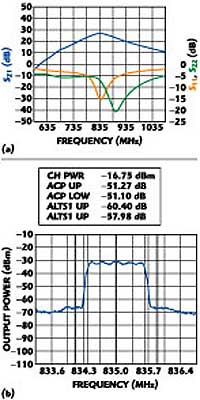
Figure 4 shows the CW performance of the NADC/AMPS PA over temperature and frequency at 3.6 V, while CDMA PA performance is shown in Figure 5.
The bandgap-reference bias scheme gives the family of amplifiers an extremely flat Pout and PAE characteristic over temperature. Lowering the supply from 3.4 V to 2.9 V (minimum voltage condition) lowers the saturated output power from 31 dBm to 30 dBm.
Ruggedness (SWR) Testing
The PA ICs described here withstand industry standard load SWR tests (SWR = 10 at all phases, Vcc = 5 V) under RF drive sufficient to saturate the PA. Without the protection circuitry, results show the PA would fail catastrophically. These results were obtained using the standard 5HP/AM (NPNHB Vceo = 5.5 V) technology along with the on-chip SWR protection circuits.
Thermal Testing
Thermal measurements were made on the output device of the SiGe PA. The results are shown in Figure 6 for a multirow power cell and for a close view of the emitter region. The measurements were obtained under full RF drive and a base temperature of +85° C. The Si substrate provides a higher thermal conductivity than GaAs (1.5 vs. 0.46 W/cm °C).7 For the production SiGe IC thickness of 200um, the junction temperatures in a standard QFN package have been shown to be less than 125°C at full CDMA power. This is considerably less than what is observed for PAs in GaAs thinned to 100 µm (two times thinner, but with three times lower thermal conductivity).
|
|

CONCLUSION
SiGe PAs are a compelling alternative to GaAs HBT PAs for a variety of reasons. The NPN device RF performance is on par with other technologies, and PA IC performance is competitive. Si technology has an advantage for high volume production because wafers are larger and process yields higher, which should lead to better availability and lower cost. Bias reference and control circuitry is more accurate due to more sophisticated schemes that are possible in BiCMOS. There is a clear path to higher integration in a BiCMOS process that is not possible in GaAs due to lack of a good selection of device types and lower yields.
To these authors' knowledge, this is the first time that SiGe PAs have withstood industry standard ruggedness tests. This performance allows the PAs to be used in handset applications, which was not previously possible.
ACKNOWLEDGMENT
The authors wish to acknowledge Chris Saint for IC layout and Teddy O'Connell for technical assistance. *
References
1. D. Greenberg, "SiGe BiCMOS Technology for RF/Analog/Mixed-signal Applications," IEEE RFIC Symposium, WSA02B Workshop, June 2000.
2. A.K. Oki, et al., "Future Trends of HBT Technology for Commercial and Defense Applications," IEEE MTT-S Symposium on Technologies for Wireless Applications Digest, 1997, pp. 123125.
3. X. Zhang, et al., "A SiGe HBT Power Amplifier With 40 Percent PAE for PCS CDMA Applications," IEEE MTT-S Symposium, June 2000.
4. P. Gray and R. Meyer, Analysis and Design of Analog Integrated Circuits, 3rd Edition, Wiley, New York, 1993.
5. S. Cripps, Power Amplifiers for Wireless Communications, Artech House Microwave Library, New York, 1999.
6. J. Yuan, SiGe, GaAs and InP Heterojunction Bipolar Transistors, Wiley, New York, 1999.
7. S.M. Sze, Physics of Semiconductor Devices, 2nd Edition, Wiley, New York, 1981.