
TECHNICAL FEATURE
Power Efficient MMIC Frequency Triplers
The design of an efficient frequency tripler for an S-/X-band communications receiver is described. An approach for optimizing the tripler for best power efficiency is presented. The tripler topology consists of the harmonic generator circuit, a bandpass filter and an amplifier. A novel tunable filter to increase the bandwidth of the tripler was fabricated and tested. Measured performance of an X-band GaAs MMIC frequency tripler is shown versus simulations.
Spacecraft in deep space missions, or even terrestrial satellites, have a limited amount of power available. It is very expensive to accelerate each pound of the spacecraft to 17,600 mph or greater. Compared to terrestrial communications equipment, space communication systems place a higher priority on small, lightweight and low power circuitry. In cases where commercially available components do not fit well with space communication designs, custom designed MMICs can often fit the small, lightweight and low power circuitry requirements for space communications. A small low power S-/X-band receiver was being developed under NASA Advanced Technology Development (ATD) funds at Johns Hopkins Applied Physics Laboratory. An early prototype of the receiver included a commercial frequency tripler module of several cubic inches that consumed 1.4 W of DC power. It was replaced with a custom GaAs MMIC frequency tripler 54 by 54 mils square dissipating 0.15 W resulting in an order of magnitude improvement in weight, size and power consumption. Using this custom GaAs frequency tripler MMIC saved size, weight and power consumption in an S-/X-band receiver module requiring a total 1.3 W of DC power -- less than the commercial tripler module alone.
An approach to optimize the power efficiency of an MMIC tripler is presented. It is based on a topology suggested previously.1 There are three basic sections of the frequency multiplier: the harmonic generation section, a filter section and an amplifier for the third harmonic.
Figure 1 illustrates the relative spectrum of the signal in each of the three sections of the tripler. In the harmonic generation section, multiple harmonics are produced with a nonlinear device (GaAs MESFET). A filter section greatly attenuates the strong fundamental and second harmonics. Higher order harmonics could be filtered in a bandpass section, but the on-chip filter is required only to filter out the first and second harmonics such that the third harmonic dominates the final amplifier stage. This topology works well for a frequency tripler and could be used for an efficient frequency doubler. This topology of a harmonic generator (MESFET at pinchoff) and filter section was used previously to produce an S-band to C-band frequency doubler.3
|
|
For this MMIC design, the harmonic generation section uses a 300 µm FET (MESFET) in TriQuint's TQTRX GaAs process. The bias of the device is near pinchoff to maximize the nonlinear characteristics for the third harmonic. This harmonic generator also produces a very strong first and second harmonic, which require filtering.
A high pass or bandpass filter is used to attenuate the unwanted harmonic components. The goal is to attenuate the second harmonic enough to keep it from saturating the output amplifier. Additional off-chip filtering can be added; however, on-chip filtering is necessary to attenuate the second harmonic by at least 20 dB. The requirement to attenuate the second harmonic while passing the third harmonic makes this topology inherently narrowband. Using a higher order filter section or a tunable filter could improve the bandwidth. A tunable high pass filter to double the practical bandwidth is described later.
The amplifier section is designed to increase the third harmonic level. A narrowband amplifier could be designed to provide additional filtering of the undesired harmonics, or the amplifier could be designed wideband with attenuation provided by on-chip or external filter sections. For these triplers, broadband efficient one-stage and two-stage amplifiers were designed to amplify the desired third harmonic (6.6 to 7.5 GHz). The two-stage amplifier was also fabricated as a separate 5.5 to 8.5 GHz efficient general-purpose amplifier.
HARMONIC GENERATION
A nonlinear device is required to generate harmonics of the input signal. For this design, a 300 µm FET in TriQuint's TQTRX process is used. The device is biased around pinchoff to enhance the nonlinear characteristics. The device was designed for a drain voltage of +5V but could also operate at +3.3V. A +3.3V supply tends to enhance the nonlinear characteristics while lowering power consumption. Bias near pinchoff is supplied to the MESFET gate through a resistor divider network decoupled from the RF matching circuit through a large inductor and large decoupling capacitor. The input matching network (IMN) to the 300 µm FET is centered around the fundamental frequency (2.2 to 2.5 GHz), while the output matching network (OMN) is optimized for the third harmonic (6.6 to 7.5 GHz). Figure 2 shows a simplified schematic of the harmonic generator. To reduce risk, the harmonic generation section used the same proven, but narrowband, design1 retuned to a higher fundamental frequency of 2.2 to 2.5 GHz. While the overall tripler is inherently narrowband, it may be desirable to design a broadband harmonic generator section. Flexibility could be gained by broadbanding the harmonic generator and output amplifier while using the filter roll-off characteristics to set the operating band of the tripler. This would allow fabrication of tripler MMICs to cover a large range of frequencies by only modifying, or tuning, the filter section for each operating band.
|
|
|

The FET biased near pinchoff generates very strong fundamental and second harmonic signals. Setting the gate bias voltage has an effect on the gain (or loss) of each harmonic generated in the FET. A typical response (simulated) of the harmonic generator section is shown in Figure 3. Note the strong first and second harmonics followed by a reasonable third harmonic and progressively weaker higher harmonics. The output of the harmonic generator feeds into the filter section.
THIRD HARMONIC FILTER
The filter section is very important to the characteristics of the tripler design and its bandwidth. This topology could also be used for a doubler by re-designing the filter to take advantage of the very strong second harmonic. As a tripler, an ideal infinite roll-off high pass filter would still only allow for a 50 percent bandwidth. The high pass roll-off of the filter must be designed to pass the third harmonic of the lowest frequency of operation but have sufficient attenuation at the second harmonic of the highest frequency of operation. Additional filtering of undesirable harmonics could be achieved in the filter design, but the primary concern is to ensure that only the third harmonic saturates the final amplifier stage. A high pass filter could be used in place of the bandpass since the harmonic generator already attenuates higher order harmonics. The size of the filter stage is important. Higher order filters could theoretically improve bandwidth but the addition of "non-ideal" elements increases loss, size and complexity.
The current bandpass filter design provides a tripler bandwidth of approximately 15 to 20 percent. External filtering could be added to the MMIC tripler to improve attenuation of unwanted harmonics. Tuning the passband frequency by replacing some of the capacitor elements with varactors can increase the bandwidth of the tripler design provided that the amplifier and harmonic generator are sufficiently broadband. The schematic of the bandpass filter is shown in Figure 4. For the tunable filter, two fixed capacitors are replaced by variable capacitors (varactors) plus some resistors and additional capacitors to supply the reverse bias voltage to the varactors. Figure 5 shows the typical response (simulated) of the fixed filter section. Figure 6 shows the response (simulated) of a tunable filter where two of the four capacitor elements are replaced by reverse biased diodes acting as varactors. The tuning range of the variable filter is approximately 15 percent, which would double the current tripler bandwidth.
|
|
|
|
| |
EFFICIENT AMPLIFIER DESIGN
For space applications, size, weight and power consumption are key criteria for the communications design. Given the limited availability of commercial triplers, this was an excellent application for a custom MMIC optimized for the frequency and RF power requirements of the system. The input signal level was assumed to be 0 to +10 dBm, and the output third harmonic level was expected to be as high as +10 or +13 dBm. The amplifier MESFETs were sized to be power efficient, capable of delivering +12 to +15 dBm. A two-stage and a one-stage amplifier were designed for the MMIC tripler. The additional gain of the two-stage amplifier was desirable, but it is riskier and more difficult to design a stable two-stage amplifier than a single stage one.
A successful MMIC tripler operating from 1.55 to 1.75 GHz was designed previously.1 One of the trade-offs in the original design was to operate a single stage amplifier at saturation to maximize the gain (IDSS ≈ 80 mA for a 300 µm FET at +7V). That design only had enough room for a single stage amplifier on the 54 x 54 mil GaAs die, so DC power was sacrificed for a higher output signal level. The amplifier is the key component in this architecture that affects power efficiency. Since little power is consumed in the harmonic generator section biased near pinchoff, the amplifier consumes the bulk of the DC power.
|
|
The output stage of the amplifier was sized based on the IV curves for the FET device with ±5V power supplies, plus a 2 dB margin. Estimating the maximum RF output power (Pout ) available in Class A from the device I-V curves is illustrated in Figure 7. Given a fixed supply voltage (Vs = +5V) and assuming a knee voltage of 1V, the maximum voltage swing is Δ V = 2 x (Vs 1), in this case ΔV = 8V. The maximum current swing (ΔI = Imax ) is proportional to the device size. Assuming a fixed voltage supply, and a sufficient device breakdown voltage, the output power is determined by the maximum current swing, that is, device size.
For an Imax greater than 100 mA, Pout is approximately +20 dBm for a 300 µm FET for a +5V supply. That would yield approximately +17 dBm for a 150 µm FET. Hence a 150 µm FET is chosen to provide 2 dB margin for a +15 dBm output requirement.
A 150 µm FET operating at approximately IDSS /2 could provide about +15 dBm, while reducing the bias to IDSS /4 could provide at least +12 dBm. To simplify the matching design, 150 µm FETs were used for the first and second stage amplifier. Bias was made selectable so that the final stage could operate at IDSS /2 (20 mA) or IDSS /4 (10 mA) depending on the output power required, while the first stage is operated at the lower IDSS /4 bias. S-parameters for the 150 µm device were not expected to vary much between IDSS /2 and IDSS /4, so the amplifier could be custom configured for either bias point. Even though the design was intended for ±5V, it works well with +3.3 and 5V supplies. External resistors could be used to optimize the bias for a ±3.3V system. A single stage amplifier was designed for 10 or 20 mA bias at +5V, while the two-stage amplifier consumes an additional 10 mA for a bias of 20 or 30 mA at +5V.
While the power efficiency of the tripler is dominated by the power consumption in the amplifier section, optimizing the size of the FET in the harmonic generator is necessary for best overall efficiency. If the output power requirement were reduced, then not only should the FETs in the amplifier be made smaller, but the FET in the harmonic generator would need to be made smaller to match the levels required by the amplifier. At some point, a compromise must be made in customizing the design to a specific requirement. It is important to build-in design margins at the cost of extra DC power in order to provide for changing specifications during development, or to make the design flexible enough that it could be used for other systems. Adding extra bond pads to make the bias selectable is one way to optimize a single MMIC design for multiple requirements. Figure 8 shows an example of modifying the gate bias by connecting to one bond pad or another. Attaching to the bond pad V1 provides a gate bias voltage of 1.25 V for a lower drain current, while attaching to V2 selects a gate bias voltage of 0.8 V for a higher drain current. Note, the 500 Ω resistor also provides RF stability for the MESFET.
|
|
AMPLIFIER DESIGN RESULTS
As mentioned, the amplifier has a strong impact on the efficiency of the overall tripler. MESFETs are sized according to the design's output power requirement plus some additional margin. Ideally, a multi-stage amplifier would have the MESFET size optimized for each stage. To simplify the matching circuit design, the same device (150 µm FET) was used for both stages in a two-stage amplifier. The first stage is run at a lower current level (~IDSS /4), while the output stage is biased for maximum class A output power (~IDSS /2). Matching circuits are designed to be sufficiently broadband. Generally, one desires the band of the amplifier to exceed the requirements for the tripler operating range so that any processing variations in the GaAs fabrication will still allow the amplifier to meet specifications. For this design, additional bias points were included that can be selected by bonding to different pads when packaged. Off-chip resistors could be added to optimize the bias points for a design that requires less output power. Each stage of the amplifier could be operated from a low of about 15 to 20 percent IDSS up to 55 to 60 percent IDSS for maximum output power. At some point, it is preferable to redesign the tripler with smaller MESFETs optimized for a lower output power requirement than to use an existing design and operate the MESFETs at too low a current bias. Given the many available papers on amplifier design and matching circuit design, a thorough step-by-step explanation of this amplifier design will not be given. Suffice it to say that the design strives to trade-off gain, stability, bandwidth, efficiency and proper de-coupling of the DC bias lines in the matching circuit design of an amplifier.
LAYOUT
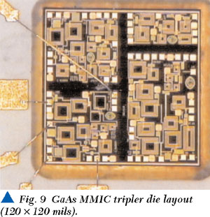
Since this was a development or "proof of concept" project, multiple variations of the tripler and amplifier circuits were combined on a single large die to maximize the knowledge gained from a single fabrication cycle. For a production run, the two-stage tripler could be produced as a single 60 x 60 mil die. A single die of 120 x 120 mils using the Prototype Chip Option (PCO) for TriQuint's TQTRX GaAs process was used. Four separate designs were fabricated on one prototype die. A single stage amplifier/tripler (2.2 to 2.5 GHz) occupied one quadrant, a two-stage amplifier/tripler (2.2 to 2.5 GHz) occupied another quadrant, a two-stage broadband efficient amplifier (5.5 to 8.5 GHz) occupied one-eighth of the die and the remaining three-eighths contained a frequency tripler (1.7 to 2.1 GHz) with a tunable filter section. ICED (IC Editors Inc.) was used for the layout and design rule checking. Figure 9 shows the actual chip with one tripler (quadrant) wire bonded into a test package.
|
|
MEASURED RESULTS
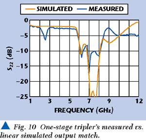
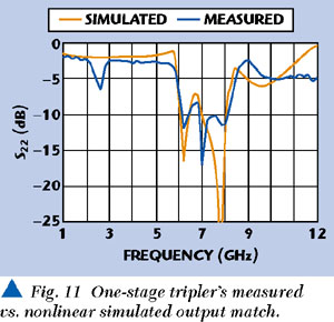
Simulated results agree well with the measured results. Agilent EEsof's Libra program was used for simulations using linear models from the TQTRX foundry manual2 and TriQuint's Own Model (TOM2 and TOM3) for nonlinear simulations. For the harmonic generator FET, the linear model with the lowest available current bias (14 percent IDSS ) was used for simulations. For the one-stage tripler, both the linear model and the nonlinear model simulations agree well with the output match, as shown in Figures 10 and 11.
|
|
|
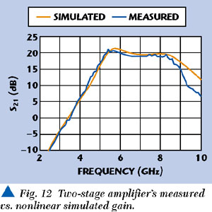
Linear and nonlinear simulations for the two-stage amplifier vary a little depending on whether the output stage bias uses the IDSS /2 bias or the IDSS /4 bias. For the input match, the linear model at low bias (14 percent IDSS ) for the 300 µm FET matched the measured result very well. At the higher third harmonic frequencies, the actual amplifier rolls off a little lower in frequency than expected. Still, the two-stage amplifier has about 20 dB gain from 5.5 to 8.5 GHz and greater than +13 dBm output power at 21 mA from the +5V supply. Gain for the simulation and measurement agrees well, though the gain roll-off occurs slightly lower in frequency than predicted, as seen in Figure 12. The power output (> +13 dBm) agreed well with estimates from the DC I-V curves and from nonlinear simulations.
|
|
|
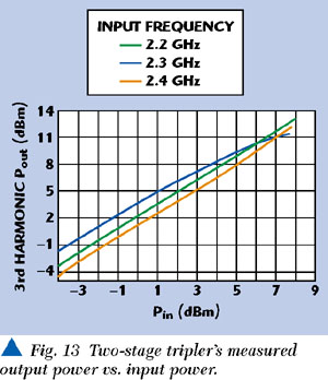
Nonlinear simulations of the overall tripler predicted a third harmonic output approximately 6 dB higher than measured results. This corresponds to the same difference as in the original design.1 Besides blaming an overoptimistic nonlinear model, the 6 dB error could also be due to the narrowband match on the input of the harmonic generator circuit. The nonlinear model predicted a better input match at the optimal frequency for the tripler than the measurements indicate. Possibly broadbanding the harmonic generator in a future design would create better agreement with the nonlinear models. Figure 13 shows the third harmonic power out versus power in at 2.2 to 2.4 GHz for the two-stage tripler. Tables 1 and 2 list measured performance for the single stage amplifier/tripler and the two-stage amplifier tripler operating at +3.3V with a 2.3 GHz input signal. The MMICs were packaged on a small aluminum block with SMA connectors attached. The measurements are calibrated at the SMA connectors.
|
|
|
|
The tunable filter produced a tuning range on the order of 250 MHz from 1.75 to 2.00 GHz. While the tunable filter worked well, the current harmonic generator design needs to be broadbanded to fully utilize the extended tuning range. The tunable harmonic generator and filter section were tested with the 5.5 to 8.5 GHz two-stage amplifier circuit while varying the control voltage. As shown in Table 3, the peak performance of the band shifts by modifying the control voltage. Bandwidth at each control voltage setting is approximately 250 MHz around the "peak" performance point. This MMIC is also tested as a packaged component.
|
|
The schematic of the variable filter was shown previously. The tuning element is a reverse biased diode formed from a MESFET with source and drain shorted together. Changing the voltage of the reverse bias on the diode modifies the capacitance from gate anode to source/drain cathode. While the relative tuning range is determined by the varactor GaAs processing, the designer chooses the nominal value of the variable capacitance by specifying the MESFET diode size. Two of the four capacitors on the fixed filter were replaced with varactors to achieve a 15 percent change in the roll-off frequency. Three additional large capacitors were added to supply the reverse bias control voltage to the varactors. The two capacitors on the input and output of the filter isolate the varactor bias from the harmonic generator and amplifier.
CONCLUSION
An architecture for frequency triplers (or doublers) in GaAs MMICs has been described and fabricated. Customization of the circuit can allow for low power efficient operation in a particular system. For space applications, size, weight and power consumption are critical. Certainly, customized MMICs with selectable bias points can provide extremely small, lightweight, low power solutions when off-the-shelf components are not available, or not suitable.
ACKNOWLEDGMENT
The author wishes to acknowledge Craig Moore, his co-teacher in Johns Hopkins University's MMIC Design Course EE787 since 1989. He would also like to acknowledge Carson Murray, who implemented a successful MMIC tripler design during the Fall 1997 semester of the MMIC Design course that proved the architecture for this tripler design. Funding for the creation of this MMIC was part of APL's Advanced Technology Development (ATD) for NASA. *
References
1. C. Murray, "Frequency Tripler," Student Reports, JHU EE787 MMIC Design Course, Fall 1997.
2. TriQuint Semiconductor, GaAs IC Deisgn Manual, TriQuint TQTRX Process, V2.0, 1997.
3. M. Reece, "Design of a S/C-band Frequency Doubler," Student Reports, JHU EE787 MMIC Design Course, Fall 2000.
|
|
 John E. Penn received his BEE from the Georgia Institute of Technology in 1980, and his MS degrees in electrical engineering and computer science from the Johns Hopkins University in 1982 and 1988, respectively. His work has involved custom integrated circuit design, silicon compilers, digital design, microwave design and microwave integrated circuits (MMICs). Mr. Penn is employed in the space department of the applied physics laboratory and co-teaches a MMIC design course with Mr. Craig Moore at the Johns Hopkins University (EE787).