
As low cost and low volume gain increasing importance in today's technology market, the development of lateral and vertical interconnects for K- through W-band applications using silicon micromachining is a worthwhile endeavor. Thus, lateral components appropriate for multi-layer applications, such as Wilkinson dividers, reactive tees and right angle bends, have been developed at 94 GHz. Wafer-to-wafer interconnects with only 0.1 dB insertion loss have also been developed in addition to vertical through-wafer interconnects with 0.5 dB insertion loss at 94 GHz. These components are integrated into a multi-layer silicon, micromachined power cube, 6 mm in length, 6 mm in width, 1 mm in height, that represents the first W-band (94 GHz) transmit module to date. The multi-layer silicon environment, with appropriate design and packaging, yields a solution to the low power problems of conventional monolithic microwave integrated circuits (MMIC) by providing more power per unit area. This article presents details of the passive components and interconnects involved for a 94 GHz design, although they may also be applied to lower frequencies.
Today's microwave and millimeter-wave markets are driving three important requirements: low cost, high performance and small size. This, in turn, dictates the replacement of traditional waveguide components, which are massive and costly but extremely low loss, with smaller semiconductor products. Solid-state device technology has driven the development of planar MMICs that dominate today's communications systems. This technology has allowed for the design of small RF circuits that combine many functions on a single circuit while providing high performance and low cost. During the past two decades, the level of integration, available materials, batch-production yields, reliability and raw performance of high frequency and high speed components have steadily increased. Consequently, many frequency and speed requirements previously met with large volume and/or weight components are now achievable with miniature, lightweight and highly reliable devices.
The semiconductor industry has been designing ICs in standard packages for more than 25 years. However, it has become clear that the performance advantages inherent to very large scale integration (VLSI) semiconductor devices will not be realized at the system level with conventional packaging.1 Consequently, many new packaging technologies have evolved at the chip-level, such as ball grid arrays, that combine a dense area of contacts with a chip surface-mount, and multi-chip modules (MCM) that integrate chip packaging. Originally MCMs allowed bare chip attachment to a printed circuit board substrate using wire bonding, tape automated bonding (TAB) or flip-chip, and eliminated individual packaging and the associated parasitics. Today a MCM substrate may be made of ceramic materials, thin films over silicon (also known as high density integration (HDI)) or printed wiring board, and may include interconnects as well as multiple chips.
|
|

Despite these advances, the development of MCM technology has clearly demonstrated the difficulty in realizing high power systems in monolithic form. The main reasons for this power limitation are low power MMIC devices, high loss interconnects and passive components, low efficiency planar antennas and limited integration capability. The need to develop MMICs with high power and low cost leads to a number of requirements for optimum high frequency performance: lightweight hardware, high density interconnect technology, high reliability and advanced packaging. The development of high power microwave circuits with both small size and low cost poses serious challenges. The response to this challenge is to use novel concepts in circuit design, fabrication and implementation to establish significant new benchmarks in power output.
A MULTI-LAYER APPROACH
The next step beyond the current state-of-the art for the presently used MCM is the development of a technology which can provide monolithic integration of silicon (Si) or silicon germanium (SiGe) circuits, advanced micro-electromechanical system (MEMS) devices,micromachined analog components (such as filter or multiplexers) and digital CMOS-based processing circuits into one wafer or multi-wafer stack. One way to meet the requirements for both the microwave market and the semiconductor industry is a multi-layer approach, as shown in Figure 1. By replacing single chips, MCMs and/or wafers with three-dimensional integration, substantial size and weight reductions may be achieved.2 For example, a four chip stack requires less printed circuit board real estate as compared to four adjacent chips, improving substrate efficiency. With regard to power, a multi-wafer stack can provide more power per unit area than a single wafer in which sources and interconnects are on the same lateral plane. In addition, reducing the interconnect length through three-dimensional integration also improves performance by minimizing signal delay. The magnitude of these various benefits depends on the vertical interconnect and three-dimensional packaging.
|
|
|
|
|
|


At lower frequencies, such as X-band, bare dice are mounted on a MCM substrate and interconnected using wire bonding, TAB, flip-chip or thin-film metallization. The MCMs are then stacked vertically using various integration techniques. Ceramic MCMs using fuzz buttons in plastic spacers and filled vias in substrates are prevalent, while another example is a HDI approach for thin-film interconnects.1,3 Note that MCM substrates may be cofired ceramic, printed wiring board or a combination of thin-film metals and dielectric materials over substrates such as silicon, diamond and metal. Thus, at X-band and lower frequencies, there are many commercially available vertical interconnects for various multi-layer schemes on a number of substrates. Beyond K-band (20 to 30 GHz), and particularly at W-band (75 to 110 GHz), this is not the case, and the examination of multi-layer approaches necessitates development of novel vertical interconnects. At microwave and millimeter-wave frequencies in particular, the added discontinuities of a vertical transition make low loss and wide bandwidth more challenging goals.
SILICON MICROMACHINING
Silicon micromachining has been applied to microwave and millimeter-wave circuits in many ways since its introduction in the late 1980s. Micromachining, or sculpting, of single crystal Si can be made by using either orientation-dependent (anisotropic) or orientation-independent (isotropic) etchants, as shown in Figure 2. Silicon micromachined, dielectric membrane supported structures, such as antennas, transmission lines and filters, have shown improved performance and have extended the operating range of planar circuits to W-band frequencies and beyond.4,5,6 In addition, silicon micromachined-based packaging provides a high isolation self-package without the need for external carriers or external hermetic shielding. This method of circuit integration provides a comprehensive technique to integrate a very large degree of functionality on a single substrate with extremely high density and at a relatively low cost. The vertically layered structure of the micromachined circuit presents an excellent opportunity for three-dimensional integration, resulting in the potential for substantial reductions in size. Micromachined circuits are an ideal way to integrate MEMS devices and provide components with performance and size advantages from 1 GHz to the terahertz regime. However, they demonstrate their greatest promise at K-band and above. Micromachining is truly an excellent integration technology with the opportunity for an order of magnitude or more reduction in the size, weight and cost of planar circuits, which can have a major impact on radar and communications applications in the military, commercial and space arenas.
Micromachining techniques can be applied to any semiconductor substrate, but the use of Si substrate layers as the foundation of the micromachined structure has major advantages in cost and the direct integration of SiGe and CMOS circuits. High resistivity Si also has mechanical, thermal and electrical properties that compare well with the best ceramics, and as a result has been successfully demonstrated as the substrate of choice in three-dimensional integrated circuits.7 Cost comparisons have been made for simple circuit applications and show one- and two-orders of magnitude cost reductions over the same circuit packaged in ceramic. Circuit integration based on micromachined fabrication technology promises to be the key to achieving the very demanding cost, size, weight and simplicity goals required for the next advances in communications and radar systems for commercial, space and military applications.
This article focuses on Si wet bulk micromachining as applied to low loss planar transmission lines and multi-layer system integration techniques for ICs. After choosing an appropriate transmission line architecture for multi-layer applications, novel lateral and vertical interconnects will be presented. Packaging issues will be addressed before applying the interconnect technology to a W-band power cube transmit module application.
TRANSMISSION LINES FOR MULTI-LAYER APPLICATIONS
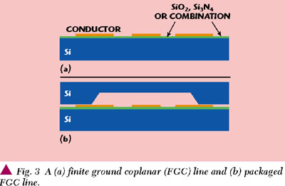
In the vertical integration of high frequency circuits, the ground conductors must follow the signal line as closely as possible in order to reduce parasitic radiation and prohibit the excitation of higher order modes. This need is exacerbated in high density architectures with multiple, adjacent vertical interconnects and lateral metallized planes. Finite ground coplanar (FGC) waveguide, as shown in Figure 3, is a uniplanar line in which ground planes and signal conductors occupy the same wafer interface thereby localizing the electric field concentration. As a result, line performance depends predominantly on line geometry and is insensitive to wafer thickness.8 The FGC line has the potential to minimize parasitic effects when transitioned vertically, and for this reason is chosen for the multi-layer interconnects described herein. The dimensions for the 50 Ω line used in this work and shown in Figure 4 are s = 40 µm, w = 24 µm, ground plane width wg = 106 µm and wafer thickness t = 100 µm. Extracting capacitance values using Ansoft's Maxwell 2-D simulator,9 the characteristic impedance is calculated to be 49.98 Ω with an effective dielectric constant equal to 6.156. To prohibit higher order mode excitation, the total width of the FGC line, WT , must be less than λg /2, where λg corresponds to the guided wavelength. At the design frequency, fc = 94 GHz, λg /2 is equal to 632 µm, a value much greater than the Wt = 300 µm implying line operation free of higher order modes.
|
|
|
|


In addition to the FGC line, micromachined finite ground coplanar (MFGC) waveguide has demonstrated significantly lower loss than conventional coplanar waveguide for frequencies up to 110 GHz.10 By simply micromachining the silicon from the aperture regions of the line, significant loss improvements can be made without sacrificing the structural integrity and without double-sided processing.10
|
|

LATERAL INTERCONNECTS
Lateral distribution of power must include low loss interconnects for division from one to two or more signal paths. For this research effort at 94 GHz, FGC-based Wilkinson power dividers and reactive tee junctions are designed for equal power division, in addition to right angle bends. Figure 5 shows the schematics of the 50 Ω designs, in which input power is split equally for 3 dB of nominal insertion loss for both the Wilkinson and the reactive tee junction. The feed line dimensions are 40 µm center conductor, 24 µm apertures and 106 µm ground planes. Note the high impedance sections under each air bridge used for compensation, and the thin-film 100 Ω resistor placed for high isolation in the Wilkinson design.
S-parameters of all interconnects presented in this article are measured on an HP 8510C network analyzer, using 150 µm pitch Picoprobes and a TRL calibration method to de-embed the probe-to-wafer transition. This method of de-embedding establishes reference planes at the input and output ports of the circuits under test.11,12
A right angle bend is added to each of the components for measurement purposes. Thus the three circuits measured for component loss extraction are the Wilkinson and bend, reactive tee and bend, and double bend. Photos of the fabricated circuits are shown in Figure 6, and measured values at 94 GHz are averaged and assigned a margin of error based on the ripple in the measurement. The attenuation of the interconnecting lines is de-embedded from the measurement and the remaining insertion loss represents that of the tested component. Table 1 shows the measured loss for each component as 0.4 dB for the Wilkinson, 0.24 dB for the reactive tee junction and 0.1 dB for the right angle bend.
|
|
|
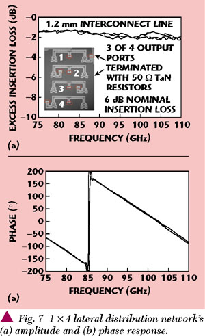

The lateral distribution network under study consists of one reactive tee junction, two Wilkinson power dividers and six right angle bends, and divides the signal from one input to four outputs.13,14 In measuring a 1:4 network, in which three of the four output ports are terminated with matched thin-film resistors, it is important to establish power balance in each of the four signal paths. Ideally, one network would be fabricated and probes would be placed on the input port and on each of the four output ports. Since this measurement set-up is unavailable, four identical 1:4 networks are fabricated and each of the four output ports is measured separately. Figure 7 shows the four measurements superimposed for insertion loss, as well as phase for 50 Ω 1:4 networks. The total interconnecting line length is approximately 1.2 mm. All four measurements match closely, with insertion loss of 1.2 dB ±0.1 dB at 85 GHz.
|
|
|
|

VERTICAL INTERCONNECTS: THROUGH-WAFER
Vertical system integration is first addressed with the development of a micromachined three-via interconnect which allows low loss transfer of millimeter-wave signals through a Si wafer. A conceptual schematic of the three-via vertical interconnect appears in Figure 8. The pyramidal shaped vias connect three-conductor transmission lines through the 100 µm thick Si substrate, and create minimal radiation into the substrate. The two ground vias open from the front side of the wafer, while the center conductor via opens from the opposite side. This allows flexibility in choosing the via separation, minimizes circuit size and reduces radiation by forcing the current to flow along the parallel inner sidewalls.
At high frequencies, compensation is required to adjust for the capacitance introduced by the vias themselves, and the inductance produced by the sharp bends in the lines. The matching network used to remedy this consists of tapered bends to smooth the transition and tuning stubs to suppress the horizontal electric field component, which contributes to radiation. In addition, air bridges are utilized for capacitive matching. Figure 9 shows the transition in a back-to-back configuration with high frequency tuning elements.
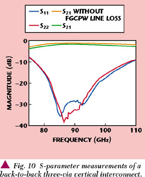
At the 94 GHz resonance of the transition, the numerically simulated insertion loss is 0.31 dB, with return loss between 26 and 40 dB.15 This result does not include conductor loss and, again, represents one three-via transition. However, it compares well with the back-to-back vertical interconnect measurement shown in Figure 10, which includes loss from the feed and midsection lines. At the slightly shifted resonance of 90 GHz, the insertion loss is 1.82 dB, with return loss at 30 dB. Since this is the loss of the feeding FGC waveguide lines, the two sets of vias and the midsection of FGC waveguide line, the loss due to the lines may be calibrated out to estimate the loss due to one vertical interconnect. At 90 GHz, the loss of the two transitions is approximately 1.1 dB. Thus the loss due to each interconnect is approximately half, or 0.55 dB.16,17
VERTICAL INTERCONNECTS: WAFER-TO-WAFER TRANSITIONS
Multi-wafer silicon designs must provide an avenue for electrical signals to flow from wafer to wafer. For this purpose, a two-layer electrical thermocompression bond is developed to provide electrical connection between two coplanar waveguides printed on the adjacent faces of two vertically stacked silicon wafers.
The thermocompression bond, at temperatures below the eutectic, compares quite favorably to classical electrical interconnects for MMIC packages or IC chips, such as wire-bonding and flip-chip technology. The 1-4 µm electro-plated transition pads are comprised of the same material as the circuit metal and thus produce little mismatch in thermal expansion at the bond temperature. The bumps do not flow during compression as would solder, and additionally, thermocompression bonds for packaging applications would yield little out-gassing for low temperature vacuum bonding as compared to solder or glass alternatives.18 Finally, thermocompression bonds of the type presented here have been tested in lap shear at the Massachusetts Institute of Technology (MIT) with strengths comparable to that of wire bonds.18 Unlike many previous wafer-to-wafer silicon-gold bond investigations, the goal of this work is not only to develop a low temperature gold-to-gold wafer bond, but to develop an RF electrical connection from one silicon wafer to another at W-band.
|
|

Figure 11 illustrates the transition concept and measurement method as a back-to-back configuration. In this measurement scheme, a single FGC line transitions from lower to upper wafer, and then back to the lower wafer for on-wafer probing. Probe windows are micromachined through the upper 100 µm wafer, and 40 µm air cavities are micromachined around the FGC line for protection. The lower (AA') and upper (CC') FGC cross sections have dimensions of 40-24-106 µm (S-W-Wg ) and line thickness of 1 µm, while the transition region (BB') includes an additional 3 µm of gold on both sides to ensure wafer-to-wafer contact. Once in contact, the gold of BB' is 8 µm in height and sandwiched between the silicon wafers, thereby changing the shunt capacitance, effective dielectric constant and characteristic impedance of the line at the transition region. To design a transition with good RF performance at W-band, the transition geometry must be modified to preserve the original 50 Ω characteristic impedance.
Electrostatic simulations show that a 50 Ω line may be achieved in the transition region while maintaining compactness with minor changes to the FGC feed line dimensions.9 Full wave analysis of the back-to-back transition with finite conductivity yields insertion and return losses of 0.85 and 20 dB, respectively, at 94 GHz.19 A simulated through line of the same length yields insertion and return losses of 0.684 and 36 dB, respectively. The difference in insertion loss is 0.166 dB, implying 0.083 dB insertion loss per transition.
|
|

At 94 GHz, the attenuation of the 50 Ω line in the transition area is 0.22 ±0.02 dB/mm. Figure 12 shows an RF back-to-back transition measurement, with return loss plotted on the left axis and insertion loss plotted on the right. At 94 GHz the insertion loss is 0.28 dB, with return loss of 30 dB. As shown in the photograph, the calibration reference planes are placed just at the transition so the insertion loss of the measurement includes the loss of two wafer-to-wafer transitions and the 400 µm midsection of feed line. Based on the known attenuation of the line, the loss of the 400 µm midsection is 0.088 ±0.008 dB. Subtracting this line loss from the total insertion loss yields 0.192 ±0.008 dB loss for the two transitions. Thus the loss per transition may be approximated as 0.096 ±0.008 dB per transition.20
PASSIVE COMPONENT INTEGRATION AND PACKAGING
In high density circuits, on-wafer packaging becomes an important means of isolating circuits while preserving performance integrity. With multi-layered configurations, the vertical stacking of substrates necessitates a thorough understanding of propagating wave effects due to the surrounding environment. Although the electromagnetic fields in FGC lines are fairly well confined to the aperture regions, it is important to further reduce interactions between adjacent circuits (laterally and vertically) in order to achieve the highest possible integration. Electromagnetic parasitic interactions, known as cross-talk, are due to substrate modes and/or proximity effects and result in degraded electrical performance. This parasitic coupling can be reduced or eliminated by appropriate shielding. Recent work has demonstrated that on-wafer packaging has the ability to effectively isolate circuits while preserving performance integrity and providing very small size and low cost solutions.21 In the vertically integrated circuits studied herein, on-wafer packaging does not only isolate adjacent circuits but provides mechanical protection to the air bridges.
|
|
|


To analyze the coupling effects in vertically integrated multi-layer transmission lines, the lateral spacing between lines is varied from 0 to 400 µm center-to-center, and cross coupling is simulated by measuring the insertion loss across two diagonal ports and leaving the remaining two ports open. Cross sections for the simulations are shown in Figure 13. Simulated results show a ripple in cross coupling (S21 ) due to parasitics for line separations of less than 300 µm.22 The level of coupling for the lines separated by 0 and 100 µm is as high as 10 dB near the design frequency. By introducing an air-dielectric layer between the metal conductors, as shown in Figure 14, the ripple is eliminated completely and the coupling level for the closest spacing reduces to 20 dB as indicated.
Thus the performance of W-band circuits may be degraded when placed in a multi-conductor environment due to strong proximity coupling. Silicon micromachined and air-dielectric shielding cavities, realized between the two, reduce the parasitic coupling and maximize propagation efficiency. This line architecture is ideal for multi-layer integrated circuits. As pertains to the following multi-layer application, shielding cavities of 40 µm are implemented and separation between vertical lines is no less than 300 µm, keeping line-to-line coupling below 50 dB.
MULTI-LAYER APPLICATION: W-BAND POWER CUBE
As a multi-layer Si application, a W-band power cube has been developed in which power from four flip-chip MMICs is distributed both vertically and laterally through three micromachined Si layers to feed a four-by-four array of patch antennas.23 This integrated circuit is intended as a 0.007 in3 (102 mm3 ) Si transmit array building block with 2 W/in2 radiated power. Silicon micromachining process technology is responsible for all passive components, which includes the interconnecting transmission lines, vertical interconnects and power distribution networks introduced in the previous sections. In addition, thermocompression bonding techniques are utilized for wafer-to-wafer interconnects and stacking of all Si layers.
|
|

As indicated in Figure 15, the input signal is divided into the four InP power MMICs through a power distribution network consisting of one reactive tee junction, two Wilkinson power dividers and six right angle bends on FGC waveguide. The four amplified output signals propagate vertically through a thinned silicon wafer using micromachined interconnects and emerge on the other side of the silicon wafer. Next, the signals are divided laterally through four additional distribution networks. Since each of the signals is divided into four, sixteen feed signals result with 6 dB of nominal loss. Vertical transmission to the next silicon layer is achieved using RF FGC bonded pads. After transitioning to this layer, the FGC line is transformed to microstrip in order to feed the sixteen aperture-coupled micromachined patch antennas in phase. The resulting transmit module is only 6 mm by 6 mm in area and 1mm in height.
|
|
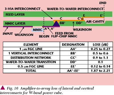
This W-band multi-layer transmit module has been designed, fabricated, bonded and partially tested at 94 GHz. In addition to the development of individual lateral and vertical interconnects, the component integration makes the power cube not only a densely integrated multi-layer circuit, but an integrated conformal package utilizing thermocompression bonding. The insertion loss from the MMIC amplifier to the microstrip array excitation is 1.8 to 2.4 dB, as shown in Figure 16. The range of values represents the error in the measurement at 94 GHz.
CONCLUSION
As multi-layer structures become a desirable means of achieving high density integrated circuits, vertical interconnects become critical to their success. Criteria upon which to evaluate a vertical interconnect include loss, bandwidth, transmission efficiency, size and ease of fabrication. Particularly at W-band, the added discontinuities of any vertical transition make low loss and wide bandwidth more challenging goals. In this article, Wilkinson dividers, reactive tee junctions and right angle bends with insertion losses of 0.4, 0.2 and 0.1 dB have been presented as lateral interconnects appropriate for multi-layer applications. In addition, wide-band through-wafer vertical interconnects with 0.5 dB insertion loss and wafer-to-wafer thermocompression-bonded vertical interconnects with 0.1 dB insertion loss have been shown. All of the interconnects presented are compact and use conventional fabrication processing. In addition, these novel interconnects have been applied toward the first W-band (94 GHz) transmit module to date. Not only is this transmit module a high density multi-layer circuit, it is also an integrated conformal package utilizing thermocompression bonding. This multi-layer silicon environment, with appropriate design and packaging, can provide a solution to the low power problems of conventional MMICs.
ACKNOWLEDGMENTS
This work was supported by DARPA/ETO (contract N66001-96-C-8635), the Office of Naval Research (contract N00014-98-1-0628) and the Army Research Office (contract DAAD19-99-1-0197). The HP 8510C network analyzer is a product of Agilent Technolgies, Santa Rosa, CA. The Picoprobes are a product of GGB Industries, Naples, FL. This article is based on material first presented at the European Microwave Conference held in Paris, October 2000. *
References
1. P.E. Garrou and I. Turlik, Multichip Module Technology Handbook, McGraw-Hill, New York, 1998.
2. S.F. Al-Sarawi, D. Abbott and P.D. Franzon, "A Review of 3D Packaging Technology," IEEE Transactions on Components, Packaging and Manufacturing Technology-Part B, Vol. 21, No. 1, February 1998, pp. 214.
3. C.L. Lassen and M.V. Christensen, "The Via Squeeze," IEEE Spectrum, Vol. 36, No. 10, October 1999, pp. 3641.
4. T.M. Weller, L.P. Katehi and G.M. Rebeiz, "High Performance Microshield Line Components," IEEE Transactions on Microwave Theory and Techniques, Vol. 43, No. 3, March 1995, pp. 534543.
5. R.F. Drayton, T.M. Weller and L.P.B. Katehi, "Development of Miniaturized Circuits for High Frequency Applications Using Micromachining Techniques," International Journal of Microcircuits and Electronic Packaging, Vol. 18, No. 3, Third Quarter 1995, pp. 217223.
6. L.P.B. Katehi, "Si Micromachining in High Frequency Applications," CRC Handbook on Si Micromachining, CRC Press, Boca Raton, FL, 1995.
7. R.M. Henderson and L.P.B. Katehi, "Silicon-based Micromachined Packages for High Frequency Applications," IEEE Transactions on Microwave Theory and Techniques, Vol. 47, No. 8, August 1999, pp. 16001607.
8. K.J. Herrick, T. Schwarz and L.P.B. Katehi, "Si-micromachined Coplanar Waveguides for Use in High Frequency Circuits," IEEE Transactions on Microwave Theory and Techniques, Special Issue on Millimeter-wave Technologies, Vol. 46, No. 6, June 1998, pp. 762768.
9. Maxwell 2D, Ansoft Version 1.9.04, 1997.
10. K.J. Herrick, T.A. Schwarz and L.P.B. Katehi, "Si-micromachined Coplanar Waveguides for Use in High Frequency Circuits," IEEE Transactions on Microwave Theory and Techniques, Vol. 46, No. 6, June 1998, pp. 762768.
11. R.B. Marks and D.F. Williams, NIST, Boulder, CO, August 1995.
12. R.B. Marks, "A Multiline Method of Network Analyzer Calibration," IEEE Transactions on Microwave Theory and Techniques, Vol. 39, No. 7, July 1991, pp. 12051215.
13. T.M. Weller, R.M. Henderson, K.J. Herrick, S.V. Robertson, R.T. Kihm and L.P.B. Katehi, "Three-dimensional High Frequency Distribution Networks-Part I: Optimization of CPW Discontinuities," IEEE Transactions on Microwave Theory and Techniques, Vol. 48, No. 10, October 2000, pp. 16351642.
14. R.M. Henderson, K.J. Herrick, T.M. Weller and L.P.B. Katehi, "Three-dimensional High Frequency Distribution Networks-Part II: Packaging and Integration," IEEE Transactions on Microwave Theory and Techniques, Vol. 48, No. 10, October 2000, pp. 16431651.
15. IE3D User's Manual, Release 5, Zeland Software Inc., Fremont, CA, 1998.
16. K. Herrick, J.G. Yook and L.P.B. Katehi "Microtechnology in the Development of Dimensional Circuits," Invited Paper, IEEE Transactions on Microwave Theory and Techniques, Special Issue on Advanced Integration Schemes, Vol. 46, No. 11, November 1998, pp. 18321844.
17. K.H. Herrick, J.G. Yook, S.V. Robertson, G.M. Rebeiz and L.P.B. Katehi, "W-band Micromachined Vertical Interconnection for Three-dimensional Microwave ICs," 29th European Microwave Conference Proceedings, Munich, Germany, October 1999, pp. 402405.
18. M.A. Schmidt, "Wafer-to-wafer Bonding for Microstructure Formation," Proceedings of the IEEE, August 1998, pp. 15751585.
19. HP 85180A High Frequency Structure Simulator, Ansoft Version 1.9.04, 1997.
20. K.J. Herrick and L.P.B. Katehi, "RF W-band Wafer-to-wafer Transition," accepted for publication in IEEE Transactions on Microwave Theory and Techniques, Vol. 48, No. 8, August 2000.
21. R.M. Henderson and L.P.B. Katehi, "Silicon-based Micromachined Packages for High Frequency Applications," IEEE Transactions on Microwave Theory and Techniques, Vol. 47, No. 8, August 1999, pp. 15631569.
22. K.J. Herrick, R.M. Henderson and L.P.B. Katehi, "Wave Effects in Si-micromachined Multilayer Guiding Structures Operating at W-band," 1999 IEEE MTT-S International Microwave Symposium Digest, Anaheim, CA, June 1999, pp. 6164.
23. K.J. Herrick, R.T. Kihm and L.P.B. Katehi, "Interconnects for a Multi-layer Three-dimensional Silicon Architecture," 30th European Microwave Conference Proceedings, CNIT, La Defense, Paris, October 2000.
|
|
 Katherine J. Herrick received her PhD in electrical engineering from the University of Michigan, Ann Arbor, in January 2000 under the guidance of Professor Linda P.B. Katehi. She received her BSE and MSE degrees in electrical engineering from the University of Michigan, Ann Arbor, in 1993 and 1995, respectively. During the 1997 and 2000 International Microwave Theory and Techniques Symposiums, she received Best Student paper awards. Her dissertation work focuses on integrated three-dimensional microwave circuits up to W-band utilizing silicon micromachining. Currently, she is conducting research as a post-doctoral research fellow in the areas of MEMS, filters and multi-layer silicon circuits.
 Linda P.B. Katehi received her BSEE degree from the National Technical University of Athens, Greece, in 1977, and her MSEE and PhD degrees from the University of California, Los Angeles, in 1981 and 1984, respectively. In September of 1984 she joined the faculty of the EECS department of the University of Michigan, Ann Arbor, as an assistant professor, and moved to the levels of associate professor in 1989 and professor in 1994. She served in many administrative positions, including director of graduate programs in the college of engineering from 1995 to 1996, elected member of the college executive committee from 1996 to 1998, associate dean for graduate education from 1998 to 1999 and associate dean for academic affairs since September of 1999. Professor Katehi has also served on numerous college of engineering and university committees.
  R.T. Kihm is a senior fellow at Raytheon Electronic Systems, El Segundo, CA, and has been with the company since 1978. He is currently working on the development of a high power Ka-band imaging radar system as the RF hardware responsible engineer. At Raytheon, previously Hughes Aircraft Co., he has had numerous assignments in the development of active MMW missile seekers. Kihm worked at the Naval Electronics Laboratory, San Diego, CA, from 1971 to 1977 developing MMW surveillance systems. He received his PhD and MSEP (electrophysics) degrees from the Polytechnic Institute of Brooklyn in 1972 and 1966, respectively, and his BSEE from the Case Institute of Technology in 1963.