
This article addresses some of the unique advantages that uniplanar technology can offer the microwave circuit designer. In contrast to the conventional microstrip approach, uniplanar techniques allow a mixture of transmission line configurations to be used together, thereby making available a wide range of novel passive microwave structures. Specific examples of the use of series and shunt elements in coplanar waveguide (CPW) are discussed and the design of a reduced size Wilkinson divider is presented.
The recent interest in new wireless applications, such as the local multi-point communications system (LMCS) and local multi-point distribution system (LMDS), is creating a demand for MMICs at high frequencies. Minimum chip size is one of the key considerations in MMIC design, and for this reason lumped elements have been very popular below 20 GHz, their small size giving them a distinct advantage over larger, distributed transmission lines. However, at higher frequencies, lumped element losses, self resonance effects and parasitics in general become significant, and lumped element components, such as inductors, are rarely used as matching elements. On the other hand, distributed circuit elements are very well understood and at high frequencies their size is less of a penalty because of the reduced wavelengths. For these reasons, accurate modeling information for lumped elements such as inductors is scarce at LMDS frequencies and a distributed design is the more common approach.
In distributed element-based MMICs, microstrip is the best understood and, therefore, the most common transmission line approach used today. However, uniplanar technologies, such as coplanar waveguide (CPW) and coplanar stripline (CPS), possess many well known advantages over microstrip for monolithic microwave and hybrid integrated circuits. These include low dispersion, insensitivity to substrate thickness, easy connection of both shunt and series elements, the ability to easily realize short circuit elements and the elimination of via holes (reducing cost and parasitic inductance). An attractive feature of CPW that is not often discussed is the fact that the characteristic impedance of CPW is governed by the ground plane separation and signal conductor track width. This means that variable geometry, constant impedance transmission lines can be fabricated easily, reducing discontinuities and allowing low parasitic interconnections and transitions to be made. Other transmission lines such as slotline, a rarely used element in today's planar microwave circuits, is also a member of the uniplanar family, and when combined with coplanar elements can offer circuit element characteristics which cannot be achieved with microstrip. Uniplanar technology can, therefore, provide the designer with the opportunity to create new circuit topologies having increased performance over classical implementations1,2 and, as a result, is becoming more attractive to the MMIC designer, particularly at millimeter-wave frequencies.
In general, the matching requirements encountered in the design of a distributed-element MMIC demand the use of both series and shunt passive elements -- series elements dictating the length of the chip and shunt elements dictating the width. This article discusses the concept of incorporating the series and shunt matching elements in the center conductor of CPW line in an effort to reduce the overall size of MMIC chips. A reduced size Wilkinson divider developed in asymmetric coplanar stripline (ACPS) is used to illustrate the flexibility of the uniplanar approach.
CENTER CONDUCTOR SERIES STUBS IN CPW
Since microstrip is the most common transmission line encountered in MMICs, the concept of a series stubs is relatively rare. Figure 1 shows the realization of a series stub located in the center conductor of CPW line, a short circuit series stub and an open circuit series stub. The electric field patterns present in the structures are also shown. Through selection of the appropriate stub termination and its length, a series inductive or capacitive reactance can be realized at the break in the center conductor. This offers a degree of circuit design flexibility not available in microstrip.
|
|
|
|

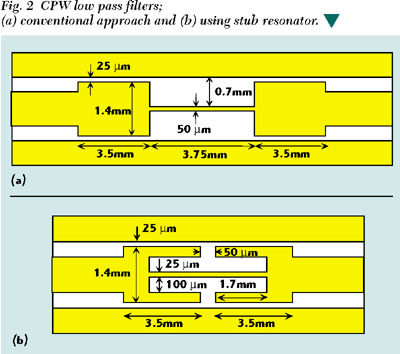
An example of how this design flexibility can be used to reduce the size of a CPW filter network is shown in Figure 2. The layout of a conventional low pass filter on alumina consists of a cascade of alternate high and low impedance line sections. This third-order filter has one inductive line (Z0 = 143 Ω) and two capacitive lines (Z0 = 26 Ω), and has a cut-off frequency of 3 GHz. The alternative configuration uses two back-to-back short circuit series stubs to form a series resonator positioned within the low impedance CPW line sections which simulate shunt capacitors. This technique of embedding some of the matching elements inside other elements allows reuse of the same physical space in one of the directions, in this case the direction of the main transmission line, and leads to a 35 percent reduction in the length of the filter. The experimental results of the conventional and compact filters are plotted in Figure 3, where it can be seen that the compact filter does not present any degradation of bandwidth. In addition, there is no shift in the cut-off frequency and the transmission loss remains lower than 0.4 dB. Finally, the compact configuration improves the behavior of the filter in the stopband region by suppressing spurious responses over a large bandwidth beyond the cut-off frequency of the low pass filter.
|
|

CENTER CONDUCTOR SHUNT STUBS IN CPW
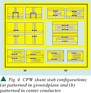
Intuitively, it is easy to visualize the realization of series stubs in the center conductor of a CPW line. CPW shunt stubs, on the other hand, are usually connected to the inner conductor but are located in spaces opened up in the ground plane. In the case of GaAs MMICs, this configuration can quickly use up valuable GaAs real estate because they are usually orthogonal to the main CPW line and are typically λ/4 in length. This waste of real estate is often compounded if two CPW lines with shunt stubs are run parallel to each other or if a single CPW line with shunt stubs is meandered in an effort to reduce the total length of the chip. However, shunt CPW stubs can also be positioned in the inner conductor, significantly freeing up valuable GaAs area on both sides of the CPW line. Figure 4 shows examples of these new types of CPW shunt stubs along with their analogous stubs printed conventionally in the ground plane. In order to allow this "folding" of the shunt stubs into the center conductor, a portion of the ground plane is introduced across the CPW line in the form of a thin strip. Inner conductor continuity is maintained using air bridge interconnects across the strip and the stubs to ground are formed within the center conductor using the new local ground point.
|
|
In comparison with conventional CPW shunt stubs, several advantages are obtained from the use of this interesting approach, including compactness (thereby providing low loss), reduction in the transverse footprint of the circuit, reduction in the number of air bridges (in the case of asymmetric CPW shunt stubs) and transverse symmetry around the center conductor.
The location of the stubs within the center conductor also leads to greater field confinement and thus lower radiation loss. Furthermore, the symmetry around the center conductor indicates that the parasitic coupled slotline mode should not theoretically be excited in these structures. (This contrasts with the conventional asymmetric shunt stub in which two transverse air bridges must be used in addition to the longitudinal air bridge to prevent the coupled slotline mode from being excited.)
To show the potential of these new CPW shunt stubs, several examples have been fabricated. Figure 5 shows the measured frequency response of single and double CPW shunt stubs along with theoretical results obtained using two different techniques: the integral equation technique solved with moment method and complex images, and the finite difference time domain (FDTD) method. These circuits are designed near fo = 30 GHz and implemented on high dielectric constant substrate (εr = 9.9 and h = 0.254 mm). The good agreement between experimental and theoretical results shows that the stubs work well in the millimeter-wave region. Dielectric and conductor losses are neglected in the theoretical analyses and this shows up as differences between the theoretical and experimental resonance frequencies.
|
|

INTEGRATION OF SLOTLINE WITH CPW
One of the disadvantages of conventional shunt stubs in CPW is that the designer is limited to an impedance range of about 30 to 80 Ω. Impedances outside this range cannot be fabricated reliably because of the small gaps required between the metal lines or cause excessive losses because of small line dimensions. However, it is often desirable to be able to realize high or low impedances (filters being an example where either very large or very small characteristic impedance levels are regularly required). In these situations, the difficulty in realizing low or high impedance levels with conventional shunt stubs constitutes a serious limitation in the design of the filter, particularly at high frequencies. While the upper limit of realizable characteristic impedance is set by manufacturing tolerances, the lower limit depends on the onset of higher order modes which occurs when the transverse dimension of the CPW stubs becomes comparable with the wavelength or with its longitudinal dimension. To overcome this difficulty, it can be advantageous to adopt the concept of shunt stubs in slotline, in which case the total line impedance can be increased significantly.
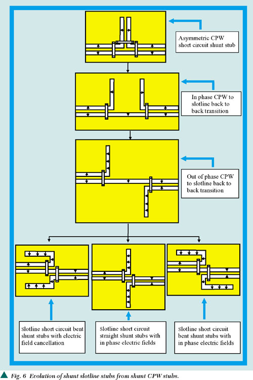
Figure 6 presents a flow chart conceptually showing how slotline shunt stubs can evolve from CPW shunt stubs. It can be seen that the slotline stub structure can also be considered as a derivation of a cascade of out-of-phase, back-to-back CPW to slotline transitions. However, when using such a structure the designer must carefully study the optimal geometric configuration of the slotline stubs. If attention is not given to the layout of the structure, the designer may find that the structure is plagued by parasitic radiation, since two slots with electric fields oriented in phase may function as a slot antenna.3,4 To minimize this problem a bent geometry is recommended so that the electric fields are out of phase, significantly reducing radiation loss.
|
|
REDUCING THE SIZE OF A WILKINSON DIVIDER
Wilkinson dividers are essential components used in many microwave and millimeter-wave circuits such as modulators, mixers, amplifiers and antenna feed networks. The standard Wilkinson divider utilizes λ/4 transmission lines, which can take up precious real estate on GaAs MMICs. Therefore, reduction in circuit size and cost is of paramount importance.
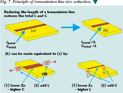
To better understand the principles of size reduction, consider the characteristics of a random length of microstrip transmission line, as shown in Figure 7. The distributed capacitance and inductance of the transmission line determine the absolute value of the line's capacitance and inductance, and these in turn determine the phase of a signal traveling along the line. If the length of the line is now simply reduced without modifying it in any other way, the total capacitance and inductance will be reduced and the phase of an electrical signal will be altered; this reduced length of line is, therefore, not equivalent to the original line. For true equivalence, its capacitance and inductance must be increased so that they are once again equal to that of the original line. This can easily be accomplished by adding lumped capacitors to ground at each end of the line and by reducing its width (effectively increasing its inductance and characteristic impedance). Alternatively, lumped inductors can be added to each end and its width increased (effectively increasing its capacitance to ground but reducing its characteristic impedance). These principles can be applied to substantially reduce the size of a Wilkinson divider.
|
|
Most examples of size reduction of couplers employ the capacitive loading approach.5 Loading the transmission line with inductors has not been as popular, probably because spiral inductors have high losses and low resonant frequencies, and require accurate models for successful design. The use of distributed elements such as short-circuit series stubs to establish the inductive loads are not common because they are difficult to realize in microstrip as discussed earlier.
The size reduction of a Wilkinson divider by the inductive loading technique has been investigated, but by employing short-circuited ACPS series stubs instead of lumped inductors. This is a good example of how some of the unique characteristics of uniplanar elements can be applied to reduce the size of a passive component while avoiding the problems associated with lumped elements. CPS transmission lines have been shown to support excellent signal propagation characteristics in the millimeter-wave frequency bands.6 CPS lines support a quasi-TEM mode and also have the advantage that, unlike CPW, they do not require ground plane interconnections (such as air bridges) at discontinuities to suppress the even mode of propagation.
A SIZE REDUCTION EXAMPLE
As stated above, one technique that has previously been used to reduce the length of transmission lines is to load each end with a lumped capacitor, C, or an open-circuit shunt stub of impedance Z0s and length  s .5 The shortened line's length and impedance are l and Z0l , respectively.
By equating the ABCD matrices of the original transmission line and the reduced length structure, shown in Figure 8, it can easily be shown that the structures can be made equivalent at one frequency if


|
|
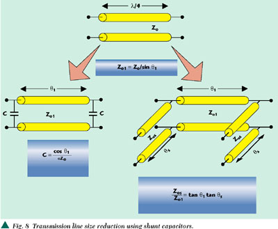
Note that by examining Equation 1, it can be seen that if the length l of the shortened line is to be less than that of the original line, that is, less than 90°, then its characteristic impedance, Z01 , must be greater than that of the original line.
With uniplanar technologies, the opportunity exists to implement both capacitive and inductive types of loading because of the ability to realize shunt as well as series distributed elements. Therefore, the possibility of achieving transmission line length reduction by using series inductors, L, or short-circuit series stubs of length s and impedance Z0s can be examined.
Equating the matrices again, it is easy to show that the series inductor topology can be equivalent to the original transmission line if
Z01 = Z0 sin 1 (4)


By examining Equation 4, it can be seen that the use of inductive loading results in a shortened line with a lower Z0 than the 90° line. Uniplanar technology allows the designer to choose the most feasible topology depending on the realizability of the required line impedance and circuit elements. A line reduction of 50 percent can be achieved by altering the original impedance by a factor of Œ„2, as shown in Figure 9
|
|

ACPS SERIES STUB TOPOLOGY
CPS lines consist of two metal strips of width W, separated by a slot of width S. ACPS lines are similar to CPS lines except that the two metallic strips are of different width. This extra degree of freedom allows for flexibility in the characteristic impedance and effective permittivity.7
In order to apply the inductive loading technique for size reduction, a physical realization of a short-circuit series stub in ACPS is required. ACPS series and shunt stubs along with other discontinuities have been previously studied.8,9 Here, the topology shown in Figure 10 (often referred to as a spur-slot discontinuity) is used. The ideal transmission line equivalent circuit used to model the structure is also shown.
|
|

In order to determine the frequency response of the ACPS series stub and the validity of using its simple equivalent circuit, a simple ACPS stub, designed to operate at 20 GHz, was simulated using Agilent's ADS Momentum™ software.10 It can be seen from S11 that the λ/4 short-circuit stub transforms the impedance to an open circuit at 20 GHz. However, looking into port 2, the structure looks like a short-circuit at 20 GHz because of the λ/4 transmission line cascaded with the stub. This response agrees well with the simple equivalent circuit. It is important to note that the Z0 of the series stub is much lower than would be the case for an isolated ACPS line of the same dimensions because of the coupling effect with the main CPS line. This limits the size reduction that can be achieved using this method.
DESIGN PROCEDURE
The topology of the Wilkinson divider/combiner is based on that presented by Jaisson, and Fan and Chang.11,12 The center frequency for the design is 22.25 GHz. The first step in the design procedure is to use Equations 4, 5 and 6 to determine the parameters of the line and stub. In this case, l was chosen to be approximately 60°, which represents a reduction in length of 33 percent. A further reduction was not attempted because it would require larger inductive loading. This, in turn, would require a higher stub Z0 , which was difficult to achieve using the ACPS series stub structure. Equations 4 and 5 yield Z0l = 61.2 Ω and L = 0.25 nH. A Wilkinson divider using these parameters was then simulated in ADS 9 using ideal elements to verify performance. This topology is shown in Figure 11.
|
|

The next step involved replacing the ideal elements with the ACPS structure described previously. Since the Wilkinson divider can be formed from four identical ACPS series stubs positioned back to back, only one had to be designed. These were then cascaded together to form the complete circuit. Initial dimensions for the line and stub were estimated from standard equations7 and an EM simulation was performed.
The resulting S-parameters were converted to ABCD parameters from which the element values could be ascertained using


The widths, gaps and lengths of the ACPS structure were then adjusted manually and another EM simulation was performed. This iterative procedure allowed optimum values for l , Z0l and L to be determined. The final circuit is shown in Figure 12. Note that in this design no effort was made to compensate for the parasitics introduced by the bends, resistor or Y connection dividing the CPW input into the two ACPS arms of the circuit.
|
|

FABRICATION AND RESULTS
The final circuit was fabricated using the in-house MHMIC process. The metal traces are gold and the resistor is TiW. The substrate used was high resistivity ( > 10,000 * cm) Si with a thickness of 400 µm. In order to facilitate on-wafer probing, one layout had port 3 directly connected to an integrated on-wafer 50 Ω resistor. Another layout was configured to allow measurement of the isolation performance. The circuit was measured using a Wiltron 360 VNA and G-S-G probes. The thru-reflect-line (TRL) calibration technique was employed and CPW standards were printed on-wafer for this purpose.
The simulated and measured results are shown in Figure 13. At mid-band the return loss and isolation is better than 22 dB, while the insertion loss is approximately 0.7 dB. Reasonably good agreement between simulation and measurement was obtained. Note that for the isolation measurement port 1 was terminated with a coaxial 50 Ω load connected to the G-S-G probe. As a result port 1 was not perfectly matched. To account for this mismatch in the simulation, the reflection coefficient of the probe and 50 Ω load was measured and included in the simulation.
CONCLUSION
Uniplanar technology has many unique advantages that can be very attractive to the microwave circuit designer. Series, as well as shunt matching stubs, can be realized and used to reduce the size of planar passive elements. The use of ACPS series stubs for the size reduction of a Wilkinson combiner/divider was presented and it was found that the design could be carried out using ideal transmission line models with good success. The 22 GHz divider example illustrated that an approximate line length reduction of 33 percent was possible; however, with further development it is thought that this could be improved to at least 50 percent.
ACKNOWLEDGMENT
This article is based on material first presented at the European Microwave Conference held in Paris, October 2000. *
References
1. K. Hettak, N. Dib, A. Omar, G.Y. Delisle and M.G. Stubbs, "A Useful New Class of Miniature CPW Shunt Stubs and its Impact on Millimeter-wave Integrated Circuits," IEEE Transactions on Microwave Theory and Techniques, Vol. 47, December 1999, pp. 23402349.
2. T. Wang and K. Wu, "Size-reduction and Band-broadening Design Technique of Uniplanar Hybrid Ring Coupler Using Phase Inverter for M(H)MICs," IEEE Transactions on Microwave Theory and Techniques, Vol. 47, February 1999,
pp. 198206.
3. B. Roth and A. Beyer, "Planar Slotline Millimeter-wave Resonators with Coplanar Coupling," Proceedings of the 19th European Microwave Conference, Madrid 1989, pp. 507512.
4. K. Hettak, J.P. Coupez, E. Rius and S. Toutain, "A New Uniplanar Bandpass Filter Using *g /2 Slotline and *g /4 Coplanar Waveguide Resonators," Proceedings of the 24th European Microwave Conference, Cannes 1994, pp. 13601366.
5. T. Hirota, A. Minakawa and M. Muraguchi, "Reduced-size Branch-line and Rat-race Hybrids for Uniplanar MMIC's," IEEE Transactions on Microwave Theory and Techniques, Vol. 38, March 1990,
pp. 270275.
6. M.Y. Frankel, J.F. Whitaker and G.A. Mourou, "Optoelectronic Transient Characterization of Ultrafast Devices," IEEE J. Quantum Electron., Vol. 28, October 1992, pp. 23132324.
7. C. Karpuz and A. Görür, "Fast and Simple Analytical Expressions for Quasistatic Parameters of Asymmetric Coplanar Lines," Microwave Opt. Tech. Lett., Vol. 9, August 1995.
8. Rainee N. Simons, Nihad I. Dib and Linda P.B. Katehi, "Modeling of Coplanar Stripline Discontinuities," IEEE Transactions on Microwave Theory and Techniques, Vol. 44, May 1996, pp. 711716.
9. Kavita Goverdhanam, Rainee N. Simons and Linda P.B. Katehi, "Coplanar Stripline Components for High Frequency Applications," IEEE Transactions on Microwave Theory and Techniques, Vol. 45, October 1997, pp. 17251729.
10. Agilent Technologies Advanced Design System v1.3, Palo Alto, CA, 1999.
11. Denis Jaisson, "An Asymmetrical Coplanar Waveguide for Use with a Coplanar Wilkinson Power Divider," Microwave Journal, Vol. 38, No. 11, November 1995.
12. Lu Fan and Kai Chang, "Uniplanar Power Dividers Using Coupled CPW and Asymmetric CPS for MICs and MMICs," IEEE Transactions on Microwave Theory and Techniques, Vol. 44, December 1996,
pp. 24112420.
|
|
 Khelifa Hettak received his Dipl Ing (with distinction) in telecommunications (1990) from the University of Algiers, Algeria, and the DEA degree in signal processing and telecommunications (1992) from the University of Rennes 1, France. He then joined the Electronics and Telecommunications Systems Laboratory at France Telecom's Ecole Nationale Superieure des Telecommunications (ENST), Brest, France, where he received his PhD degree in signal processing and telecommunications (with the highest distinction of the doctoral panel) in 1996. In January 1997, he joined the Personal Communications Staff of INRS-Telecommunications, a research center of the University of Quebec, Canada, as researcher, where he was involved in research and development projects on Wireless Systems for Direct Access to Subscribers and Millimeter-wave LAN on optical fiber backbone for future Broadband Indoor Wireless Personal Communication Systems supported by Bell-Quebec/Nortel/NSERC and Canadian Institute for Telecommunication Research (CITR), respectively. He joined the electrical engineering department of Laval University in October 1998 as an associate researcher, where he was involved in RF aspects of smart antennas. Since August 1999, he has been with Terrestrial Wireless Systems Branch at the Communications Research Centre (CRC), Ottawa, Canada, as a research scientist. He is involved in developing MMICs at 60 GHz, low temperature cofired ceramic (LTCC) packaging and RF MEMS switches. His research activities include the development of new millimeter-wave technologies for telecommunications and detection systems, integrated smart antennas for wireless systems, design of various microwave/millimeter-wave integrated circuits, numerical methods and indoor radio propagation channel characterization. Dr. Hettak was awarded the France Telecom Scholarship during his studies.
  Malcolm G. Stubbs received his BEng, MEng and PhD degrees from the University of Sheffield, England, in 1970, 1972 and 1976, respectively. From 1975 until 1978 he worked at the Communications Research Centre (CRC), Ottawa, Canada, under a National Research Council Post-Doctoral Fellowship Program and then moved to the Allen Clarke Research Centre (Caswell), England, where he was engaged in research into GaAs MMICs. In 1981, he returned to CRC where he is currently responsible for the development of planar microwave and millimeter-wave circuits. His interests include the modeling and application of MMICs, MEMs and LTCC technologies to high frequency components for communications systems.