
Philips Semiconductors
Foxboro, MA
Cellular infrastructure providers are ramping up plans to augment present GSM systems with a new Enhanced Data rate for GSM Evolution (EDGE) GSM system. This new format adds additional challenges to the design of the RF amplifiers used in basestation equipment. Designers must meet the traditional specifications for their amplifiers -- those of gain, gain flatness, input return loss and efficiency. However, EDGE GSM involves a complex modulation scheme, which requires that the designer meet the additional specifications of output RF spectrum (ORFS) and error vector magnitude (EVM). Tuning the amplifier circuit to optimize for one parameter often adversely affects the behavior of another. It is also paramount that the circuit maintains good performance when operated in the standard GSM format.
This article describes the results of a class AB demonstration circuit using a BLF1820-70 LDMOS transistor. This device utilizes second generation LDMOS technology with gold top metallization. The device contains integrated input and output matching, which enables an amplifier design with high gain and good gain flatness over the band of interest. The device is available in both a standard as well as an earless package.
SPECIFICATION CONSIDERATIONS
EDGE GSM uses a 3¼/8-8PSK modulation scheme. In order to maintain communications integrity and high data rates, the amplifier must not add excessive distortion to any symbol constellation point. This is quantified in the European Telecommunications Standard Institute (ETSI) specifications by a modulation accuracy specification. An EVM is defined which describes how large the error vector between any transmitted symbol and the ideal symbol point in the constellation can become without being detrimental to system performance. This definition is shown in Figure 1.

One EVM value of particular interest is the RMS EVM level. The ETSI specifications allow for an RMS EVM of 7 percent through the active line-up. A smaller EVM value must be achieved for any single stage, so that there is enough margin when cascading stages together to meet the ETSI requirement. A final stage RMS EVM value of 2.5 to 5 percent is suitable for line-ups that incorporate predistortion. Typically, if the amplifier line-up does not use predistortion, the EVM for the final stage must be held below 2 percent.
Amplifiers must also meet linearity requirements -- a measure of how much power is transmitted, undesirably, in the channels closest to the main carrier. For CDMA systems, the adjacent channel power ratio (ACPR) is the measure of an amplifier's linearity. The analogous measure for EDGE GSM linearity is output RF spectrum (ORFS). The power in a small integration bandwidth in the main channel is compared to the power in small bands which are offset from the carrier from anywhere between 100 and 6000 kHz. Figure 2 shows a hypothetical EDGE GSM spectral plot with power being integrated at the center of the carrier, and at 30 kHz bands ±400 kHz from the carrier. Table 1, from the ETSI specifications, shows the ORFS requirements at each of the break frequencies for DCS1800 band basestations.


For simplicity, the ORFS performance at only the 400 kHz break frequency will be presented in this article. The requirement at 400 kHz appears to be one of the most difficult to meet; therefore, it is convenient to choose this as a break frequency at which specification compliance must be shown.
The ETSI specifications require a 56 dBc ORFS at the 400 kHz break frequency using amplifiers supporting 8-PSK modulation (EDGE). This specification must be met at the antenna output, so some margin is necessary at the output of a final amplification stage. A 59 dBc ORFS performance at the 400 kHz break frequency is taken as the design goal for the demonstration circuit. This will allow enough margin to meet the system requirement when inputs are provided by typical driving stages, and when other equipment, such as circulators, filters or combiners, follows the amplifier line-up.
AMPLIFIER PERFORMANCE
Table 2 lists the typical performance of the BLF1820-70 amplifier obtained in an EDGE GSM application circuit. The RF performance of the BLF1820-70 in an application circuit optimized for a compromise in performance of both the EDGE and standard GSM formats in the DCS1800 band is displayed graphically. The powers indicated in the graphs for EDGE GSM performance are the average power during the bursted slot of the EDGE GSM frame.

Figure 3 shows the power gain of the amplifier when operated in EDGE GSM mode as a function of output power and frequency. A gain of approximately 12.5 dB is maintained over the power drive-up from 29 to 44 dBm, with approximately 0.2 dB of gain expansion occurring at the higher end of the drive-up.
|
|
|


Figure 4 shows the maximum RMS EVM and average RMS EVM obtained as a function of output power and frequency. It should be noted that the EVM performance of the amplifier was significantly lower than both the 7 percent specification value and the 2.5 to 5 percent design goal level for amplifiers using predistortion. The EVM performance is also better than the 2 percent requirement for amplifier line-ups that do not incorporate a predistorter.
Figure 5 shows the ORFS performance of the demonstration circuit as a function of output power and frequency. The horizontal line at 56 dBc shows the maximum allowable ORFS level in the specification. The demonstration circuit maintains considerable margin below both this specification level and the 59 dBc design goal.
|
|
|


Figure 6 is the standard GSM mode gain as a function of output power and frequency. Figure 7 shows the standard GSM mode drain current and corresponding efficiency at a 26 V drain voltage. This becomes important as the system operators will require the use of the circuitry in both EDGE GSM and standard GSM modes.
|
|
|


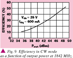
Figure 8 shows the power gain as a function of output power and frequency when the circuit is operated in CW mode. Figure 9 shows the circuit drain efficiency as a function of output power under CW conditions.
CONCLUSION
As cellular providers begin rolling out EDGE GSM infrastructure, it is important that their equipment simultaneously meet the system specifications for both EDGE and standard GSM formats. A demonstration circuit has been presented that meets these specifications using the BLF1820-70 70W LDMOS transistor. The results show that the specifications can be met with considerable margin. This will give the amplifier designer freedom to trade off the performance of one parameter for increased performance of another. For a complete application note describing the use of the BLF1820-70 for EDGE GSM applications, contact Scott Blum at Scott.Blum@Philips.com.
Philips Semiconductors,
Foxboro, MA (508) 851-2258.
Circle No. 300