
The need for bandwidth, driven primarily by the explosive demand for information transfer and communication services, has necessitated the push to microwave and millimeter-wave frequencies. While silicon-based semiconductor devices dominate lower frequency electronics, high speed compound semiconductor technologies, such as gallium arsenide (GaAs), are the enablers for such capabilities as wireless communications, local-multipoint distribution systems (LMDS) and high speed data transfer (for example, fiber optics). The next generation of these systems, as well as new systems such as automotive radar, will require even better transistor frequency responses.
High speed is attained in transistors through the use of materials that allow electrons to travel at much greater velocities than in silicon. One of the work horses in GaAs technology, the pseudomorphic high electron mobility transistor (PHEMT), uses a layer consisting of indium, gallium and arsenic (InGaAs) to provide electrons with high speed conduction. Unfortunately, the indium that gives the PHEMT its enhanced transport properties also introduces imperfections due to strain. Therefore, channels with indium mole fractions greater than approximately 25 percent are not typically fabricated on GaAs substrates, as shown in Figure 1. Historically, indium phosphide (InP) met the small, primarily military and space-based performance needs required of higher indium content channels. InP overcomes the strain induced performance limitation since it is lattice matched with 53 percent mole fraction InGaAs channels. However, the technology is expensive due to manufacturability issues associated with fabrication of the InP HEMTs, along with the lack of high quality large diameter (4" or greater) InP substrates.
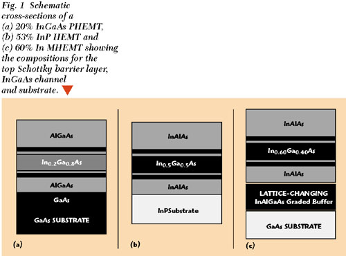
Recently, GaAs-based metamorphic HEMT (MHEMT) technology has emerged as an attractive, low cost alternative to InP HEMTs. The strain-induced imperfections caused by high indium content channels on GaAs are eliminated in MHEMTs by providing a properly grown buffer between the substrate and active device layers. With this limitation overcome, it is now possible to provide the superior performance of InP-based HEMTs (high speed, low noise and low DC power dissipation) with the cost advantages of highly manufacturable 4" and 6" GaAs wafers.
In the MHEMT, the device active layers are grown on a strain-relaxed, compositionally graded, metamorphic buffer layer which transforms the lattice constant from GaAs up through InP, allowing a high In content channel layer to be grown on low cost GaAs substrates. Additionally, the buffer layer provides the ability to tailor the lattice constant to any indium content channel desired (20 percent to > 70 percent), and therefore allows the device designer an additional degree of freedom to optimize transistors for high frequency gain, power, linearity and low noise. For example, using a metamorphic buffer layer, InP-based high electron mobility transistors (53 percent In) can be grown on GaAs substrates for a substantial cost reduction and manufacturability improvement over InP-substrate based devices.15
High In content Inx Ga1x As channel MHEMTs (x = 53 to 60 percent) have shown impressive results, achieving noise performance comparable to InP HEMTs with excellent linearity. These devices have been used to fabricate low noise amplifiers through 94 GHz, including a state-of-the-art Ka-band low noise amplifier (LNA). Using the unique ability of metamorphic technology to fabricate devices with intermediate (33 to 43 percent) In contents, high on- and off-state breakdown voltage, large power densities and 1.4 W output power amplifiers at 44 GHz have been realized.
The current status of metamorphic HEMT technology is reviewed, including low noise and power devices, as well as amplifiers fabricated from these components. This article reviews the material properties, processing, and device and amplifier performance of metamorphic HEMTs with 30 to 60 percent indium channel content.
MATERIAL PROPERTIES
The metamorphic buffer layer68 serves two purposes: to transform the lattice constant from that of the GaAs substrate to that of the high In content device active layers, and to trap lattice dislocations and prevent them from propagating into the device's channel layer. The transmission electron microsope (TEM) cross-sectional image, shown in Figure 2, illustrates the growth of an intermediate indium content HEMT (33 percent In) directly on GaAs using a metamorphic grading layer. The dislocations (shown as dark lines in the TEM) are indeed trapped in the grading layer and propagate parallel to the substrate's surface, not vertically into the device's active layers. The MHEMT's layer interfaces remain atomically smooth despite having twice the indium content and five times the total thickness as a typical GaAs PHEMT, demonstrating that metamorphic technology can successfully transform the lattice constant from GaAs.

There are distinct tradeoffs that occur as one adds In content to the channel of a (metamorphic) HEMT. Figure 3 shows the mobility of an electron traveling in the Inx GaAs channel plotted using measured room temperature Hall data, and the quantum well's depth (conduction band discontinuity) is calculated from photoluminescence measurements. The 300 K mobility of In0.56 GaAs HEMT grown on a GaAs substrate measured within 5 percent of the mobility of an identical structure on an InP substrate,7 demonstrating the high quality of the MHEMT channel. The channel electron mobility increases with indium in the InGaAs channel, due mainly to a fall in effective mass. This reduction in mass results in higher channel electron velocity, which increases ft (frequency at which the current gain goes to 0 dB) for a fixed 0.15 µm gate length, as shown in Figure 4.
|
|
|
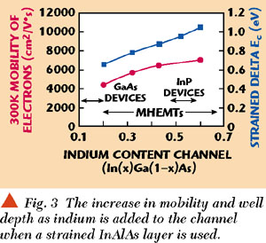
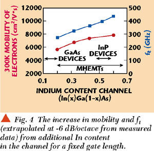
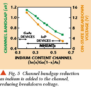
Figure 5 shows the drop in on-state breakdown with increasing indium, due to a reduction in the channel's band gap. Through the use of a strained In(Ga)AlAs Schottky layer with higher Al content and a band gap of greater than 1.7 eV, a larger conduction band discontinuity can be engineered. This provides even better quantum well confinement of the electrons and less parallel conduction, as well as improved off-state breakdown. (The displayed calculations are using this strained In(Ga)AlAs layer to calculate delta Ec .) The combined effects of improved channel mobility and larger conduction band discontinuity result in lower overall noise figure, especially at higher frequencies.
While GaAs PHEMTs and InP HEMTs are limited to In compositions near their lattice spacing, MHEMTs have a wide range of lattice constants that are available, and therefore enable the customization of the device's properties specific to each application. Although thin strained channels can be grown on InP, these metamorphic devices contain nearly 1000 angstroms of strained material, making their growth impossible without a graded buffer layer. The data points shown, some of which lie within the PHEMT's and InP HEMT's forbidden channel indium content regions, are devices which exploit this additional degree of freedom.
DEVICE PROCESSING AND LOW NOISE DC PERFORMANCE
MHEMT devices are typically mesa etched for isolation using a sulfuric- or phosphoric-based etchant. A series of metals containing Au/Ge are evaporated and annealed on the semiconductor to form an ohmic contact, with contact resistance numbers in the range of 0.08 to 0.20 -mm. Following ohmic formation, gate etching is performed by selectively removing the InGaAs cap layer and stopping on the InAl(Ga)As barrier layer. Ti/Pt/Au gates are then evaporated. Finally, silicon nitride is used to passivate the device. The device processing is nearly identical to the GaAs PHEMT process, allowing for easy integration into the GaAs production line.
The DC performance data for an In0.60 Ga0.40 As MHEMT device shows a Gm of 850 mS/mm, an Imax of 630 mA/mm, a Vpo of 0.75 V and a Vdg BRK = 8 V. An excellent uniformity of less than 3.1 percent standard deviation for all parameters across a 3" wafer is due to both the high selectivity of the gate etch and the precision of the molecular beam epitaxy (MBE) growth process.
LOW NOISE DEVICES AND CIRCUITS
The MHEMT low noise results shown here9,10 rival the best published MHEMTs11 , as well as the best InP HEMTs.12 A 0.15 µm In0.60 GaAs MHEMT biased at 1 V and 90 mA/mm showed 0.24 dB minimum noise figure (Fmin ) with 16.2 dB associated gain (Gassoc ) at 12 GHz, and 0.61 dB Fmin with 13.8 dB Gassoc at 26 GHz. Rohdin et al.11 showed 0.25 dB with 15 dB Gassoc at 12 GHz, using a 0.1 µm In0.53 GaAs/InAl0.48 As MHEMT.
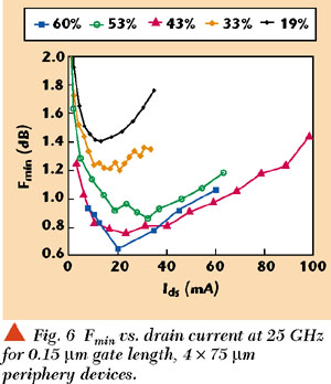
Figure 6 shows the first results of a comprehensive study on noise figure versus the channel In content of MHEMTs for 4 finger, 75 µm gate-width devices biased at Vds = 1V. As the channel In content is increased from a PHEMT's 19 percent In to a substrate-forbidden 33 percent In MHEMT, the 25 GHz minimum noise figure is reduced from 1.4 to 1.2 dB. Further increasing In content to 43 percent In results in a substantial drop in minimum noise figure to 0.75 dB. Beyond 43 percent In, no significant improvement in noise figure is achieved at 25 GHz, as demonstrated by the 53 percent In MHEMT with a Fmin = 0.85 dB and the 60 percent In MHEMT with a Fmin = 0.65 dB. Devices with shorter unit gate width resulted in lower gate resistance and Fmin s as low as 0.45 dB at 25 GHz with the 43 percent In MHEMT.
The associated gain at the minimum noise match for the same 300 µm devices is plotted versus drain bias at 25 GHz in Figure 7. The PHEMT shows approximately 8 dB Gassoc near its minimum Fmin , in contrast to the 33 percent In MHEMT with 10 dB. The 43 percent In MHEMT has ~10 to 11.5 dB of Gassoc over the large current range where noise figure remains quite low. The 53 and 60 percent devices reach their peak associated gain of 12 to 12.5 dB quickly, demonstrating the clear advantage of high indium channels at very low currents. This particular property is often exploited when building very low DC power consumption low noise amplifiers for space applications.

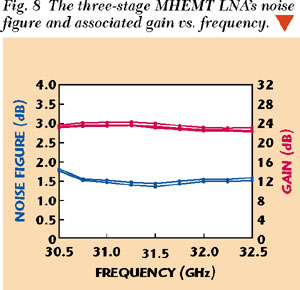
Figure 8 shows the noise figure and gain of a 3-stage 60 percent In MHEMT Ka-band LNA with less than 1.5 dB noise figure and greater than 23 dB of associated gain from 31 to 32 GHz.13 Particularly impressive is the 15 mW of total DC power consumed by this 3-stage LNA.
POWER DEVICES
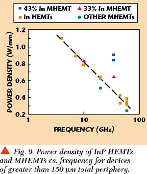
Drain bias limits of 3.5V have hampered the output power density of some MHEMT devices and most InP HEMTs, predominately due to low on-state breakdown governed by the small band gap of their high indium content channels. Even so, output power(s) (densities) of 1 W at 950 MHz,14 509 mW/mm at 20 GHz15 and 240 mW/mm at 60 GHz16 have been achieved with 53 percent In MHEMT devices. Figure 9 compares various published MHEMT results versus the best InP HEMT power devices (> 150 µm in total gate periphery), most of which consist of composite channels (InGaAs/InP) to improve on-state breakdown. The 30 to 45 percent In MHEMT devices lie considerably above the trend line, and show promise as a high power mm-wave device alternative to InP HEMTs. The 43 percent In device has also demonstrated 1.5 dB improved Gassoc at the same power output density as a GaAs PHEMT. Both devices were biased at 5 V, class AB and power tuned at 35 GHz.
Exploration of lower indium contents has resulted in higher on-state breakdown, enabling 5 V and 6 V drain biasing to be used for higher power density. Using a 33 percent In channel, > 820 mW/mm at 10 GHz17 and > 640 mW/mm at 35 GHz18 have been achieved with 6 V drain biasing. With a 43 percent In, 12 * 50 µm (600 µm) MHEMT, over 900 mW/mm was achieved at 35 GHz using a double recess structure for improved breakdown.19 Interestingly, this same 43 percent In device (with lower electron sheet density) displayed < 0.6 dB Fmin at 25 GHz due to its high channel mobility and excellent confinement. Recently, a 8.16 mm 3-stage 44 GHz power amplifier was fabricated using a 33 percent In MHEMT and demonstrated 1.4 W output power, 18 percent power added efficiency (PAE) with 14 dB of gain. It is believed that this is the highest Pout achieved on an MHEMT to date and should improve with a second iteration.
RELIABILITY
Recent work on metamorphic FET device reliability has resulted in excellent results with mean-time-to-failure (MTTF) equal to that of InP FET devices. Wakita et al.20 demonstrated 7 * 107 hours MTTF at 125°C for a 15 percent reduction in Idss using a 53 percent In MHEMT on GaAs. Recent data demonstrated > 1 * 106 hours MTTF at 125°C for 10 percent reduction in Gm and > 1 * 107 hours MTTF at 125°C for 15 percent reduction in Idss using a 60 percent In MHEMT biased at 1 Vds and 75 mA/mm (Figure 10). This initial data demonstrates the feasibility of this cost-effective, high speed metamorphic technology with reliability results that are comparable to commercial InP HEMTs.

CONCLUSION
Metamorphic HEMTs have distinct advantages over existing GaAs and InP HEMT technology: the freedom to choose virtually any high In content InGaAs channel provides for application specific device optimization and high frequency performance, while the GaAs manufacturing economies of scale (high volume, large wafer size) reduce the cost. With low noise and high frequency gain comparable to InP HEMTs, metamorphic HEMTs show promise as the next RF technology of choice to fill the emerging need for high speed communication. Metamorphic technology provides the capability for fabricating other electronic devices, such as metamorphic heterojunction bipolar transistors (M-HBT), onto GaAs substrates, allowing for higher order integration of components and device technologies onto a single chip.
ACKNOWLEDGMENTS
The authors would like to acknowledge the support of Chris McCarroll, Dave Laighton and David Van Buren, who are critical to the success of Raytheon's MHEMT program. We would also like to thank P. Buhles, M. Grigas, T. Kennedy, P. Lemonias, S. Lichwala, P. Lyman, J. Mosca and N. Pisiello, all members of the Metamorphic Development Team. The material for this article was first presented at the European Microwave Conference held in Paris, October 2000. *
References
1. A. Cappy, Y. Cordier, S. Boollaert and M. Zaknoune, "Status of Metamorphic Inx Al1-x As/Inx Ga1-x As HEMTs," 1999 GaAs Integrated Circuit Symposium, pp. 217220.
2. M. Kawano, T. Kuzuhara, H. Kawasaki, F. Sasaki and H. Tokuda, "InAlAs/InGaAs Metamorphic Low Noise HEMT," IEEE Microwave and Guided Wave Letters, Vol. 7, No. 1, 1997, pp. 68.
3. M. Chertouk, H. Heiss, D. Xu, S. Kraus, W. Klein, G. Bohm, G. Trankle and G. Weimann, "Metamorphic InAlAs/InGaAs HEMT's on GaAs Substrates with a Novel Composite Channels Design," IEEE Electron Device Letters, Vol. 17, No. 6, 1996, pp. 273275.
4. D. Gill, B. Kane, S. Svensson, D. Tu, P. Uppal and N. Byer, "High Performance, 0.1 µm InAlAs/InGaAs High Electron Mobility Transistors on GaAs," IEEE Electron Device Letters, Vol. 17, No. 7, 1996, pp. 228230.
5. S. Bollaert, Y. Cordier, V. Hoel, M. Zaknoune, H. Happy, S. Lepilliet and A. Cappy, "Metamorphic In0.40 Al0.60 /In0.40 Ga0.60 As HEMT's on GaAs Substrate," IEEE Electron Device Letters, Vol. 20, No. 3, 1999, pp. 123125.
6. W.E. Hoke, P.S. Lyman, J. Mosca, C.S. Whelan and A. Torabi, "Growth and Characterization of Metamorphic Inx (AlGa)1-x As/Inx Ga1-x As High Electron Mobility Transistor Structures with X = 0.30.4," J. Vac. Sci. & Tech. B, May/June 2000.
7. W.E. Hoke, P.J. Lemonias, J.J. Mosca, P.S. Lyman, A. Torabi, P.F. Marsh, R.A. McTaggart, S. M. Lardizabal and K. Hetzler, "MBE Growth and Device Performance of Metamorphic High Electron Mobility Structures Fabricated on GaAs Substrates," J. Vac. Sci. & Tech. B, 17 (3) 1999, pp. 11311135.
8. Y. Cordier, S. Bollaert, M. Zaknoune, J. diPersio and D. Ferre, "AlInAs/GaInAs Metamorphic HEMT's on GaAs Substrate: From Material to Device," 10th International Conference on Indium Phosphide and Related Materials, May 1998, pp. 211214.
9. C.S. Whelan, S.M. Lardizabal, W.E. Hoke, P.F. Marsh, R.A. McTaggart and T.E. Kazior, "A Comparison of Channel Indium Content in Low Noise Metamorphic HEMTs with Inx Ga1-x As (0.3<X<0.6)," InP and Related Materials 2000.
10. P.F. Marsh, S.L.G. Chu, S.M. Lardizabal, R.E. Leoni III, S. Kang, R. Wohlert, A.M. Bowlby, W. E. Hoke, R.A. McTaggart, C.S. Whelan, P.J. Lemonias, P.M. McIntosh and T.E. Kazior, "Low Noise Metamorphic HEMT Devices and Amplifiers on GaAs Substrates," 1999 Microwave Theory and Techniques Symposium, Vol. 1,
pp. 105108.
11. H. Rohdin, A. Nagy, V. Robbins, C. Su, C. Madden, A. Wakita, J. Raggio and J. Seeger, "Low Noise High Speed Ga.47 In.53 As/Al.48 In.52 As 0.1-µm MODFETS and High Gain/Bandwidth Three-stage Amplifier Fabricated on GaAs Substrate," Seventh International Conference on Indium Phosphide and Related Materials, 1995, pp. 7376.
12. P.C. Chao, A.J. Tessmer, K.G. Duh, P. Ho, M. Kao, P.M. Smith, J.M. Ballingall, S.M.J. Liu and A.A. Jabra, "W-band Low Noise InAlAs/InGaAs Lattice-matched HEMTs," IEEE Elect. Dev. Letters, Vol. 11 (1), 1990.
13. P.F. Marsh, S. Kang, R. Wohlert, P.M. McIntosh, W.E. Hoke, R.A. McTaggart, S.M. Lardizabal, R.E. Leoni III, C.S. Whelan, P.J. Lemonias and T.E. Kazior, "Millimeter-wave Low Noise Metamorphic HEMT Amplifiers and Devices on GaAs Substrates," 1999 GaAs IC Symposium, pp. 225228.
14. W. Contrata and N. Iwata, "Double-doped In0.35 Al0.65 As/In0.35 Ga0.65 As Power Heterojunction FET on GaAs Substrate with 1 W Output Power," IEEE Electron Device Letters, Vol. 20, No. 7, 1999, pp. 369371.
15. D. Tu, S. Wang, J.S.M. Liu, K.C. Hwang, W. Kong, P.C. Chao and K. Nichols, "High Performance Double-recessed InAlAs/InGaAs Power Metamorphic HEMT on GaAs Substrate," IEEE Guided Wave Letters, Vol. 9, No. 11, pp. 458460.
16. M. Zaknoune, B. Bonte, C. Gaquiere, Y. Cordier, Y. Druelle, D. Theron and Y. Crosnier, "InAlAs/InGaAs Metamorphic HEMT with High Current Density and High Breakdown Voltage," IEEE Elect. Dev. Letters, Vol. 19, No. 9, 1998, pp. 345347.
17. C.S. Whelan, W.E. Hoke, R.A. McTaggart, P.S. Lyman, P.F. Marsh, R.E. Leoni III, S.J. Lichwala and T.E. Kazior, "High Breakdown Voltage InAlGaAs/In0.32 Ga0.68 As Metamorphic HEMT for Microwave and mm-wave Power Applications," 1999 MTT, Vol. 3, pp. 11871190.
18. C.S. Whelan, W.E. Hoke, R.A. McTaggart, P.S. Lyman, P.F. Marsh, S.J. Lichwala and T.E. Kazior, "High Power and Gain at 35 GHz Utilizing an InAlGaAs/In0.32 Ga0.68 As Metamorphic HEMT," 1999 GaAs IC, pp. 221223.
19. C.S. Whelan, W.E. Hoke, R.A. McTaggart, S.M. Lardizabal, P.S. Lyman, P.F. Marsh and T.E. Kazior, "Low Noise In0.32 (AlGa)0.68 As/In0.43 Ga0.57 As Metamorphic HEMT on GaAs Substrate with 850 mW/mm Output Power Density," IEEE Elect. Dev. Letters, January 2000.
20. A. Wakita, H. Rohdin, V. Robbins, N. Moll, C. Su, A. Nagy and D. Basile, "Low Noise Bias Reliability of AlInAs/GaInAs MODFETs with Linearly Graded Low Temperature Buffer Layers Grown on GaAs Substrates," Tenth International Conference on Indium Phosphide and Related Materials, 1998, pp. 223226.
|
William E. Hoke is manager of research and production of III-V epitaxial materials at Raytheon RF Components. He received his PhD from the University of Illinois in 1978 and then joined Raytheon Company. At Raytheon his work has involved developing materials for device applications, including HgCdTe photodetectors, GaAs IMPATT diodes, GaAs PHEMTs, GaAs HBTs, InP HEMTs and metamorphic HEMTs. His current interests are developing advanced MHEMTs, phosphorus-based MBE growth and nitride materials.
K.C. Hwang received his PhD in electrical engineering from the University of Florida, Gainesville, FL, in 1990. That year he joined the Electronics Laboratory, General Electric Company, Syracuse, NY, where he developed state-of-the-art low noise and power InP-HEMTs up to 94 GHz, in addition to PHEMTs. He was relocated to Sanders, a Lockheed Martin Company, in Nashua, NH, in 1996, and developed state-of-the-art low noise and power MHEMTs for frequencies of 2 to 94 GHz, besides working on GaN. At Sanders, he was responsible for setting up six-inch GaAs fabrication lines. In October 2000, he joined Advanced Device Research Lab, Raytheon, where he is currently working on MHEMT and GaN. He has authored or co-authored more than 30 publications and presentations. Thomas E. Kazior received his PhD from MIT. He is currently the manager of Raytheon's Research Lab with interests in GaN and MHEMTs. He has published in numerous publications.
|
 Colin S. Whelan received his BA and Master of engineering degrees in physics and engineering physics from Cornell University in 1996 and 1997, respectively. After graduating, he worked in Digital Semiconductor's research group evaluating and implementing advanced process tools in their Si fab. He is currently a senior scientist at Raytheon's Advanced Device Center, Research Labs, leading the development of Metamorphic HEMTs.
 Phil F. Marsh received the BS degree and MS degrees in electrical engineering from Montana State University in1982 and 1985, respectively. He received the PhD EE in III-V device research with the University of Michigan SSEL in 1997. Later in 1997 Phil joined the research group at Raytheon RF Components in Andover, MA, where he is developing MHEMT device and fabrication technology for low noise amplifier applications.
  Steven M. Lardizabal received his BSEE and MSEE degrees from the University of South Florida in Tampa, FL, and received a PhD degree in electrical engineering from USF in 1997. Since joining Raytheon RF Components in 1997, he has been involved in the development of Metamorphic HEMT low noise amplifier design from 1 GHz through 110 GHz. He is engineering lead for Raytheon's development of wideband high dynamic range MHEMT LNAs for ONR. Dr. Lardizabal's responsibilities include the development of active device models and noise theory for MMIC design and measurement.
  Robert E. Leoni III received his BS, MS and PhD degrees in electrical engineering and his BS degree in physics from Lehigh University, Bethlehem, PA, in 1992, 1995, 1998 and 1993, respectively. He is currently a senior scientist at Raytheon Advanced Device Center, where he concentrates on metamorphic HEMTs.