
Because of the poor thermal conductivity of GaAs, successful power MMIC amplifier design in coplanar technology requires careful thermal considerations. The influences of the active device geometry and mounting conditions have been investigated theoretically and experimentally to provide reliable thermal management design data. Fifty-µm substrate thinning and flip-chip mounting with thermal bump attachment on aluminum nitride (AlN) or diamond heat sinks exhibited temperature rises of the order of 50°C and 40° to 30°C, respectively, leading to significant improvement in the performance of coplanar power devices and circuits. These results demonstrate the potential of coplanar MMIC technology for high power applications.
In the past three years, the market for wireless communication systems operating in the 20 to 60 GHz frequency range has greatly expanded. Satellite links and multipoint distribution services (LMDS and MVDS) are being implemented at Ka-, Q- and V-band to provide subscribers with communication services such as telephone, video and Internet. These commercial applications have created a demand for watt-level GaAs power MMIC amplifiers. In contrast to microstrip amplifiers that have demonstrated high output power with good thermal properties1 , the coplanar waveguide (CPW) technology has not been considered up to now for power applications. This results from the poor power handling capabilities of CPW on GaAs caused by the absence of via-holes and close backside process, which contribute significantly to heat removal in microstrip circuits. However, because of its technical and technological advantages, coplanar GaAs MMICs have proven to be cost-effective for volume production.2 However, with modern mounting and packaging solutions like the flip-chip (FC) technique, the thermal limitations of CPW can now be overcome.
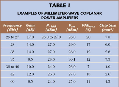
In this article, based on rigorous numerical analyses and measurements, the design issues in the thermal management of coplanar MMIC power amplifiers, such as transistor geometry, chip size and different mounting conditions, from device to circuit level, are discussed. All the coplanar MMICs presented here were designed and fabricated in-house, using a double *-doped AlGaAs/InGaAs/GaAs pseudomorphic high electron mobility transistor (PHEMT) process with 0.15-µm T-gates on 3" and 4" wafers.3 A rigorous design methodology, including thermal considerations, is the key to achieve the range of output power and reliability for the coplanar MMIC amplifiers reported in Table 1.
THERMAL CONSIDERATIONS IN COPLANAR MMIC DESIGN
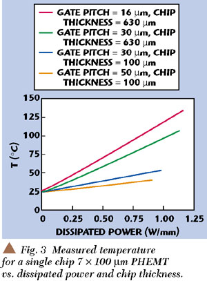
As illustrated in Figure 1, the intrinsic device performance of a coplanar PHEMT, such as the transconductance Gm and the drain current Id , are strongly dependent on the device temperature. In this case, the device is a 6 * 100 µm coplanar PHEMT (die size 2 * 2 * 0.625 mm3 ) mounted on a thermally controlled chuck. In consequence, the temperature effects have a strong impact on the achievable RF power performance of the device, as shown in Figure 2, where the measured gain (G), output power (Pout ) and power added efficiency (PAE) are plotted as a function of the chuck temperature. It can be noticed that one loses approximately 0.5 dB in both gain and output power, as well as 3 points of PAE per 25 K temperature increase. In coplanar technology, the FET temperature profile depends considerably on the device geometry (gate-to-gate spacing, source island interconnect) and the mounting conditions (on-wafer or single-chip die, chip thickness, conventional faceup or flip-chip attachment to a heat sink4 ). Figure 3 shows that different gate-to-gate spacings lead to significant temperature rises at the FET level for a chip soldered to a copper carrier on chuck. However, even if the larger gate pitch reduces heating in order to minimize the device parasitics, pitches below 30 µm should be used in millimeter-wave applications. The figure also shows that in conventional faceup (conv. FU) mounting, the substrate thickness plays a major role as well -- thinning a chip to 100 µm leads directly to a lower thermal resistance, and thus a better operating temperature with respect to the dissipated power.
|
|
|
|
|


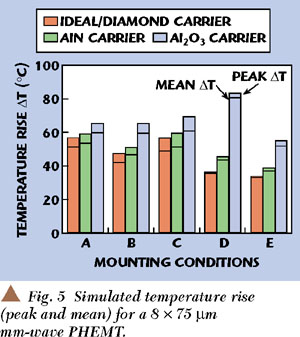
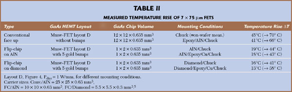
For an 8 * 75 µm FET in a single die form (2 * 2 mm2 ), the simulated temperature rises ΔT for the different layouts and mounting conditions shown in Figure 4 are illustrated in Figure 5 when the dissipated power is 1 W/mm. Compared to a 635 µm thick diced FET in conv. FU mounting (ΔT > 100°C), the 100 µm or 50 µm substrate thinning (cases A, B) lower the temperature rises to 58° and 50°C, respectively, for an attachment on aluminum nitride (AlN, thermal conductivity  = 180 W/m K), whereas the use of alumina is less effective (Al2 O3 , = 30 W/m K). In flip-chip mounting, the thermal management realized by using two big gold bumps closely placed to the outer sources (case C) of an 8 * 75 µm FET is near to that obtained with a 100 µm substrate thinning (case A). However, much better heat dissipation is achieved using smaller bumps (20 * 60 mm2 ) directly placed on the internal source islands (cases D and E), with temperature rises of only about 45°C on AlN and below 40°C on diamond (used only as reference). Table 2 shows the measured temperature rise for different mounting conditions of an 8 finger * 75 µm FET, when one finger is replaced by a temperature sensor.4 Because very good agreement between measurements and simulations for seven active fingers was achieved,5 it is possible to perform meaningful simulations under unchanged boundary conditions for eight active fingers. The extrapolated values when all the FET fingers are active are given in parentheses; for similar mounting conditions, they agree well with those of this simulation (case D, FC/AlN and Table 2, lines 3 and 4) and with the data published by C.P. Wen, et al.6 The first line from the table indicates that the on-wafer characterization of 635 µm thick wafers or large chips does not represent a worst case scenario because the large lateral dimensions play a significant role in the heat dissipation. This confirms the full three-dimensional nature of the heat flow in coplanar waveguide ICs. As demonstrated by the measurements, the best results are those obtained with flip-chip on diamond (lines 5 and 6). However, acceptable thermal management (ΔT ≈ 40°C) is also achieved using a chip flipped with thermal gold bumps on AlN (lines 3 and 4, approximately equivalent to a 50 µm thinned FU chip placed on a heat sink). Furthermore, in comparison with chips only mounted or flipped on AlN, lower temperatures are achieved using an AlN/epoxy/copper assembly, which leads to an even better thermal attachment to the heat sink.

EXAMPLES OF MILLIMETER-WAVE COPLANAR MMIC AMPLIFIERS
In addition to rigorous layout design, the power amplifier (PA) optimization is based on the load line approach considering general and loop stability, gain, bandwidth and output power. The input, inter-stage and output matching networks have the task of transforming the 50 Ω impedances from the RF ports to the very low impedances of the power devices. However, the coplanar technology faces the problem that the conventional characteristic impedance range is limited to approximately 30 to 70 Ω. In CPW, low impedance transmission lines were realized using multi-finger or capacitively loaded transmission lines.7 For both, as well as for basic passive elements, broadband models have been derived from test structures and validated up to and above W-band.8,9 The following two examples illustrate the success of this global coplanar power amplifier design strategy.
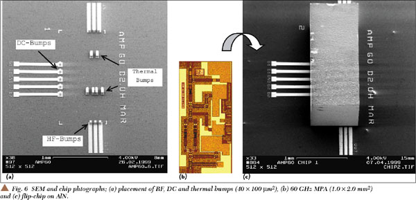
FLIP-CHIP MOUNTING OF 60 GHZ MEDIUM POWER AMPLIFIER
For applications at 60 GHz, medium power amplifiers (MPA) using optimized 4 * 60 µm devices were designed and fabricated, as shown in Figure 6. The temperature profiles of the FETs embedded in the MMIC were calculated by means of thermal simulations, on-wafer and flip-chip with or without thermal bumps. For the power levels and the devices considered here, two bumps placed close to each transistor improve significantly the temperature profile in flip-chip mounting. Figure 7 shows the effects of the thermal bumps on the MPA performance. In one case, flip-chip mounting without thermal bumps leads to a significant reduction in both gain and output power because the power is only dissipated through the RF and DC bumps. With an appropriate mounting with thermal bumps, the amplifiers reach the expected saturated output power of 200 mW at 60 GHz, with more than 10 dB linear gain and 21 percent PAE. In addition, due to the low parasitics of the optimized flip-chip interconnects, the small signal S parameters, shown in Figure 8, remain almost identical to those obtained on-wafer, resulting in a predictable amplifier behavior either on-wafer or in a flip-chip package.
|
|
|
|
|


HIGH POWER KA-BAND AMPLIFIER
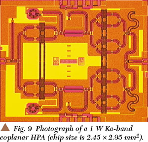
To demonstrate the potential of the coplanar technology for high power applications at Ka-band, a compact (2.45 * 2.95 mm2 ) two-stage high power amplifier (HPA), shown in Figure 9, has been developed. At 35 GHz, and at a drain voltage of 3.25 V, this HPA has demonstrated on-wafer, a linear gain of 9.5 dB and the highest output power ever reported at Ka-band for coplanar MMIC, namely a power at one dB compression (P1 dB ) of 725 mW and more than 1 W of saturated output power (Psat ), as shown on Figure 10. To verify the benefit of realistic mounting solutions (50 µm chip mounted or flipped with thermal bumps on a AlN carrier), an equivalent reduction of the temperature profile, performed using a thermally controlled chuck, demonstrated an increase in performance with a linear gain of 10.4 dB, P1 dB = 950 mW and Psat = 1.2 W.10

CONCLUSION
Active device geometry, mounting conditions and their influence on the temperature profiles and performance of coplanar power devices and circuits have been investigated and verified experimentally, providing a reliable thermal management design database. This resulted in the successful design and characterization of a number of compact coplanar MMIC amplifiers, having high output power in the 20 to 60 GHz frequency range, and demonstrated the potential of coplanar technology for power applications.
ACKNOWLEDGMENTS
The authors would like to acknowledge the valuable contributions of H. Greschbach and H. Richter (Alcatel SEL, Stuttgart), their colleagues from the technology department. This work was supported by the German Ministry of Education and Research (BMBF). W. Marsetz and Y. Baeyens are now with Infineon Technologies (Munich, Germany) and Lucent Technologies (Murray Hill, USA), respectively. This article is based on material first presented at the European Microwave Conference held in Paris, October 2000. *
References
1. J.J. Komiak, et al., "3 Watt Ka-band MMIC HPA and Driver Amplifier Implemented in a Fully Selective 0.15 µm Power PHEMT Process," IEEE MMT-S International Microwave Symposium Digest, 1998, pp. 4548.
2. M. Schlechtweg, et al., "Coplanar Millimeter-wave ICs for W-band Applications Using 0.15 µm Pseudomorphic MODFETs," IEEE Journal of Solid-state Circuits, Vol. 31, No. 10, October 1996, pp. 14261434.
3. T. Jakobus, et al., "E-beam T-gate Technology for Pseudomorphic HEMTs on 3"-GaAs with Gate Length of 0.15 µm," MANTECH Symposium Digest, 1998, pp. 169172.
4. W. Marsetz, et al., "Investigation of the Layout and Packaging on the Temperature of GaAs Power PHEMTs," Proceedings of the 28th European Microwave Conference, 1998, pp. 439442.
5. W. Marsetz, "Thermische und Elektrische Konzeption von GaAs-HEMTs für Leistungverstärker bis 80 GHz," PhD Dissertation, ISBN 3-18-331109-7, VDI Verlag, Düsseldorf, 1999.
6. C.P. Wen, et al., "Coplanar Waveguide-based, Dielectric Coated Flip-chip Monolithic Microwave Integrated Circuit, a Paradigm Shift in MMIC Technology," IEEE Millimeter-wave Monolithic Circuits Symposium Digest, 1995, pp. 123126.
7. Y. Baeyens, et al., "Miniaturized GaAs PHEMT Power Amplifiers at Ka- and Q-band Using Capacitively Loaded Coplanar Transmission Lines," Proceedings of the 28th European Microwave Conference, 1998, pp. 132137.
8. A. Bessemoulin, et al., "Capacitive Transmission Lines in Coplanar Waveguides for Millimeter-wave Integrated Circuit Design," IEEE Microwave and Guided Wave Letters, Vol. 9, Nov. 1999, pp. 450452.
9. W.H. Haydl, et al., "Models of Coplanar Lines and Elements over the Frequency Range 0 to 120 GHz," Proceedings of the 26th European Microwave Conference, 1996, pp. 9961000.
10. A. Bessemoulin, et al., "Ka-band High Power and Driver MMIC Amplifiers Using GaAs PHEMTs and Coplanar Waveguides," IEEE Microwave and Guided Wave Letters, Vol. 10, December 2000, pp. 534536.
|
|
 Alexandre Bessemoulin was born in Toulouse, France in 1971. In 1993 and 1994, he received the BSc and MSc degrees in electrical engineering from the University of Paris. From 1995 to 1998, he was with the Laboratory of Instruments and Systems. His research treated modeling of coplanar elements for high frequency integrated circuit design. Upon the completion of his PhD, he joined the Fraunhofer Institute for Applied Solid-State Physics (IAF) in Freiburg, Germany, designing power MMICs for millimeter-wave applications. His main research interests are in the area of modeling of active and passive III-V components, and high frequency integrated circuit design. He is currently the leader of the high frequency integrated circuit group at IAF.
  Waldemar Marsetz was born in Krappitz, Poland in 1968. He received the masters degree in electrical engineering from the University of Karlsruhe, Germany, in 1995 and his PhD degree from the Fraunhofer Institute for Applied Solid-State Physics (IAF) in Freiburg, Germany in 1999. His main research interest was the development of thermally optimized high frequency GaAs power amplifiers. Currently he is with Infineon Technologies in Munich, Germany, where he is involved in the development of RFICs for high data rate Wireless LAN.
  Yves Baeyens received the MS and PhD degrees in electrical engineering from the Catholic University of Leuven, Belgium, in 1991 and 1997, respectively. His PhD research was performed in cooperation with IMEC, Leuven, Belgium, and treated the design and optimization of coplanar InP-based dual-gate HEMT amplifiers, operating up to W-band. After a one and a half year stay as a visiting scientist at the Fraunhofer Institute for Applied Physics, Freiburg, Germany, he is currently a technical manager in the High Speed Electronics Research Department of Lucent Technologies/Bell Laboratories in Murray Hill, NY, USA. His research interests include the design of mixed analog-digital circuits for ultra high speed lightwave and millimeter-wave applications.
  Ricardo Osorio is a PhD student in the microsystem simulation group at IMTEK, Freiburg, Germany. He studied electrical and electronic engineering with the main subject high frequency electronics and received the Diplom-Ingenieur degree in 1995 from the Karlsruhe University, Germany. In 1995 he joined the research division of III-V devices and integrated circuits at the Fraunhofer Institute for Applied Solid-State Physics (IAF) in Freiburg, working in the area of large signal modeling of modulation-doped heterostructure field effect transistors (HFETs). He is now engaged in the investigation and modeling of electromagnetic influences in micro electronic and mechanical systems (MEMS).
  Hermann Massler was born in Radolfzell, Germany in 1965. He studied electrical engineering at the Technical University Karlsruhe, where he graduated in 1993. While working on his diploma degree at the Kernforschungszentrum Karlsruhe (KfK), he did quasi-optical measurements at 140 GHz. He continued these studies as a research assistant in the KfK for one more year. Since 1994 he has been with the Fraunhofer-Institute für Angewandte Festkörperphysik in Freiburg working on transistor- and IC-characterization up to 120 GHz.
  Axel Hülsmann was born in Dortmund, Germany in 1959. He studied solid state electronics and received the Diplom degree from the Technical University of Aachen in 1986. Since 1987 he has been with the Fraunhofer Institute of Solid-State Physics (IAF) in Freiburg, where he originally worked on optical and e-beam lithography for III/V semiconductor devices. He received his Dr.-Ing. degree from the Technical University of Munich in 1993. Currently he is responsible for the department III/V-Technology with the Fraunhofer-IAF in Freiburg working on all kinds of HEMTs on GaAs, InP and GaN and the technology of MMICs fabrication.
  Michael Schlechtweg was born in Kassel, Germany in 1958. He received his Dipl.-Ing. degree in electrical engineering from the Technische Hochschule Darmstadt in 1982, and the Dr.-Ing. degree from the University of Kassel in 1989. His dissertation treated bias dependent and nonlinear modeling of microwave FETs using a table-based large signal model. Since 1989, he has been with the Fraunhofer Institute for Applied Solid State Physics (Fraunhofer IAF) in Freiburg, Germany, where he first worked on the design and characterization of microwave and millimeter-wave integrated circuits in coplanar waveguide technology, and on nonlinear characterization and modeling of active RF devices. In 1994, he became head of the device simulation and modeling group at Fraunhofer IAF. Since 1996, he has been head of the high frequency devices and circuits department, which is focused on the design and the characterization of devices and integrated circuit based on III-V compound semiconductors for high frequency applications. The major working area is the development of monolithically integrated circuits for sensor and communication systems up to 200 GHz, and for optical high speed optical data transmission with data rates up to 40 Gbit/s. Michael Schlechtweg received the Fraunhofer Prize in 1993, and the European Microwave Prize in 1998. He has authored or co-authored more than 100 scientific publications and holds two patents.