
A fully integrated dual-frequency voltage control oscillator (VCO) for 5.2 and 5.8 GHz wireless local area network (LAN) application, providing not only a high frequency local oscillator (LO) signal to transceiver mixers but also a half-LO-frequency signal to a phase lock loop (PLL), is described. The VCO circuit has a 1.2 GHz tuning range at 7 GHz, 25 dB suppression of the fundamental frequency (3.5 GHz) signal at the 7 GHz port, and more than 20 dB suppression of the 7 GHz-signal at the 3.5 GHz port. The VCO chip was packaged and mounted on a board for phase noise measurements. A phase noise of better than 80 dBc/Hz at 100 kHz offset frequency was obtained. This work eliminates the use of frequency dividers, which reduces chip size, power consumption and cost.
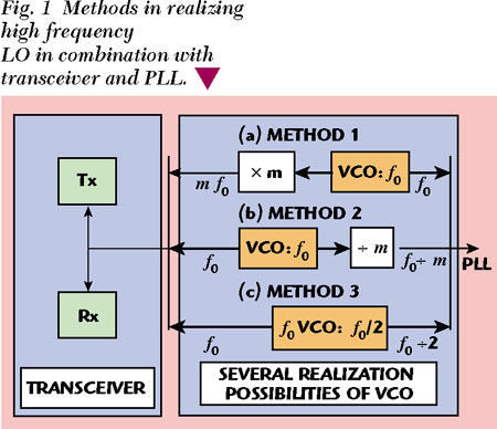
The advent of wireless communications has fueled a demand for low cost, high performance integrated circuits. Fully integrated RF transceivers are a common interest. Transceiver chips are required more and more to contain LOs, which provide a local oscillator signal not only to the transceiver but also to an off-chip PLL. However, most of the currently available PLL products in the commercial market cannot handle a LO frequency higher than 3 GHz. For a LO frequency much higher than 3 GHz an extra frequency divider is always required, as shown in Figure 1, Method 2. Another conventional solution is to multiply a LO signal at a lower frequency acceptable by a commercial PLL and using a doubler or a tripler to feed into the transceiver (Method 1). In both cases, however, the chip area and power consumption are increased. The signal with either divided or multiplied frequencies has additional phase noise due to the white noise introduced by additional active devices in the divider or multiplier and their operation within a strong nonlinear region. In addition, more design uncertainty is associated with more circuit blocks. Another technical drawback of the fundamental LO is that the low Q-factors at high frequencies severely limit the phase noise performance of a LO.
On the other hand, interest in wideband integrated LOs, covering more than one desired frequency band, is also increasing in order to significantly cut down the cost of a communication system. A typical solution is to have a single VCO that operates over a wide frequency range.1 However, this approach increases the design complexity. Although ring oscillators can provide a multi-range frequency due to their tuning ability,1 their highest operation frequencies and phase noise performance at gigahertz frequencies are limited.
This article describes a single push-push VCO circuit for wideband wireless application, which provides not only a high frequency LO signal to transceiver mixers but also a half-LO-frequency signal to a PLL (Method 3). This eliminates the use of frequency dividers, which reduces chip size, power consumption and cost. This circuit is intended to be used in an RF front end, as shown in Figure 2, for wireless LAN operating at 5.2 and 5.8 GHz. The intermediate frequency (IF) in this case was determined to be 1.45 GHz using the results of mixer spurious signal analysis. In order to avoid spurious signals falling in the passband, the VCO frequency was chosen above the RF signal, covering both 5.2 and 5.8 GHz. Therefore, not only a much higher VCO frequency but also a much wider tuning range are required than for most of the other reported work for similar applications.25 The design is based on a Philips OMMIC 0.5 µm GaAs PHEMT technology with an fT of 25 GHz.

PRINCIPLE OF A SINGLE-FREQUENCY PUSH-PUSH OSCILLATOR
Push-push topology has been employed in the past.69 According to the literature, they were realized mostly based on distributed components and at millimeter-wave frequencies. One of its advantages is that it doubles the fundamental frequencies so that higher operating frequencies can be achieved beyond the limitation caused by the cut-off frequencies of available technologies. A block diagram of a single-frequency push-push circuit is given in Figure 3.

A single-frequency push-push VCO operates simultaneously as an oscillator, a frequency doubler and a filter. It is a balanced circuit containing two identical and symmetric sub-circuits. The phase coupling network is for even-mode suppression. The output network serves as a matching network between active devices and load. Furthermore, these two networks together must be designed to make the circuit satisfy the oscillation conditions and present a negative-resistance at the fundamental frequency at the load port. The second-harmonic signal can be coupled from a fundamental virtual-ground node in the output network to the load (RL ). Therefore, twice the fundamental-frequency, twice the frequency range and low frequency pulling can be obtained for millimeter-wave applications. However, the phase-coupling and output networks were mostly realized using distributed components, which are strongly dependent of operating frequencies. As a result, their frequency range is limited. In the 5 GHz frequency range, all components can be integrated by using on-chip lumped elements. Consequently, better tuning performance is expected.
CIRCUIT DESIGN
In this case, although the operation frequency is not limited by present technologies, the concept of a push-push technique is applied here not only for a broader frequency tuning range but also for dual-frequency -- fundamental and second harmonic -- generation. From the system point of view, when the second harmonic is used as the LO signal, interference from other close-by frequency signals in a transceiver (especially in a transmitter) with the fundamental oscillation frequency can be significantly eliminated.
The circuit diagram is based on a Colpitts structure, as shown in Figure 4. The active devices FET1 and FET2 are biased with constant current sources I1 and I2 , respectively. The oscillator operates at its fundamental frequency (fo /2) determined by the two identical resonant circuits. Even harmonic signals at nfo (n = 2, ...) can be generated in phase at a fundamental virtual-ground node, doubling the frequency range and presenting a high loaded Q (QL ). This improves the frequency pulling performance and phase noise. The fundamental signal fo /2 can be coupled to an off-chip PLL directly from a differential-node pair in the circuit, which simplifies the system architecture (that is, no need for an extra divided-by-2 circuit), reduces current consumption and chip size. The drains of the FETs are connected via inductive loads to the power supply, which is designed to compensate for decreasing loop gain at the higher end of the desired frequency band. Since they are apart from the resonant circuits, the requirement for a high Q is not critical.

Two identical LC circuits composed of integrated spiral inductors of 1.4 nH at 3.5 GHz and on-chip varactor diodes of 2.1 pF (zero-biased) are designed at the fundamental frequency fo /2. Due to the technology-related limitation in metallization thickness, wide strips were chosen to enhance the Q of the inductors. A three-level metal system is used for the spiral inductors with a total thickness of 2.46 µm. Figure 5 shows the lumped-element model of the inductor with its parameters listed in Table 1. It must be noted that this lumped-element model is only valid for non-DC simulations since the substrate elements Rsub1 and Rsub2 are in parallel with Csub1 and Csub2 . Schottky barrier diodes are employed as varactors with their fingers as short as possible within the validity of the diode model. The Q of the varactor diodes was simulated and measured to be between 4 and 6 within the varactor tuning range, as shown in Figure 6. Its value is obviously not an optimal solution for VCO performance. The high series resistance is due to the size of the electrode compared with the channel thickness. The capacitance of the varactor diode is 1.56 to 3.24 pF with a tuning voltage range of 1.6 V. Furthermore, in order to have a wider frequency tuning range, two instead of one variable capacitors are introduced in the resonant circuits. A grounded resistor (R) connecting to a fundamental virtual-ground node results in even-mode suppression. Therefore, no even-mode oscillations at the fundamental frequency can occur.


A block diagram of the complete VCO is given in Figure 7. The core VCO is directly connected to a buffer amplifier A, which feeds a PLL working at fo /2, and an LC high pass filter for suppressing the possible leakage of the signal at fo /2 resulting from asymmetry of the circuit due to process variation. The simplified schematic of A is shown in Figure 8. Buffer A weakly couples a differential signal at fo /2 using two small metal-insulator-metal (MIM) capacitors, amplifies it, then gives a single-ended output signal at the same frequency to a 50 Ω load (PLL input) using a current-reused output stage. For lower transmit/receive crosstalk and higher reverse isolation, the second harmonic signal (fo ) is first fed into the high pass filter, then amplified, converted from single-ended to differential by buffer B and is later split into buffers C and D working at fo . The figure also shows the schematics of B, C and D. Buffer B refers to Q1 . Buffers C and D refer to Q2 /Q5 and Q3 /Q4 , respectively. Since the second-harmonic signal level is much lower than the fundamental, the buffers B, C and D should be designed with enough gain. Good linearity is also important for these buffers in order to lower the residual phase noise added to the core VCO output signal. In addition, C and D transfer the split differential signals into the transceiver mixers; therefore, they should be optimized to realize on-chip matching to the transmit and receive mixer input impedance, respectively. Careful circuit design considerations, such as tuned loads and variation compensation, are incorporated to improve the output voltage swing and maximum value available of the buffers under the low supply voltage.


The circuit was integrated together with a complete transceiver and was designed to operate at a frequency (fo ) of 7 GHz with a 1.20 GHz tuning range. This includes extra margin in frequency range to cover not only the 5.2 and 5.8 GHz bands but also the frequency drift caused by process variation, which can tremendously lower the yield. In order to achieve high performance with low cost, the circuits were designed using the Philips OMMIC 0.5-µm GaAs PHEMT process with 25-GHz fT . The supply voltage VDD was chosen to be 3.3 V for mobile operation.
MEASUREMENT
On-wafer measurements at ambient temperatures of 30° and 80°C were carried out. During the measurement, an external control voltage is used to compensate Idss variation. The measured frequency vs. tuning voltage of core VCOs is shown in Figure 9. The circuit has more than 1.2 GHz tuning range. The bigger difference between simulation and measurement in the frequency vs. tuning voltage curves, observed at around Vtune = 0.5 to 0.9 V, is due to the unexpected shift of the Cv vs. Vtune . The measurement confirmed the simulated output power to the PLL, as shown in Figure 10. Buffers B C and D, however, consume 15 to 18 mA more than the simulated value to deliver the same power (4.0 dBm) as used in the simulation of the mixers. The main reason is that the behavior of enhanced-mode FETs which are available only in buffers C and D deviates much more from their modeling at higher frequencies than the rest of the circuit where only depletion-mode FETs are used. The measurement shows 25 dB suppression of fundamental frequency (3.5 GHz) signal at the 7 GHz port, and more than 20 dB suppression of 7 GHz signal at the 3.5 GHz port.


The core VCO and buffers consume 10 mA and 35 mA, respectively. Although the circuit was designed to operate with 3.3 V, it performs within a wide range of supply voltage (1.8 to 3.8 V). A photograph of the complete VCO is given in Figure 11. The size of this chip is 2.0 * 1.75 mm2 .

The complete VCO has been packaged and mounted on a board together with a PLL. The packaged VCO locked by the PLL was measured in order to obtain the phase noise performance. The phase noise at various offset frequencies from the carrier can be measured by changing the bandwidth of the loop filter. The board was designed to eliminate unwanted couplings. No unexpected phenomenon caused by the package was observed compared to the bare-die on-wafer measurements. In this case the direct measurement of phase noise at the fo outputs of buffers C and D was impossible since the complete VCO was integrated together with the entire transceiver. Alternatively, the RF output of the transmitter mixer was measured. It was observed that the phase noise at both RF and fo /2 outputs is approximately 80 dBc/Hz at 100 kHz offset frequency from the carrier. The phase noise difference between these two outputs is much less than a theoretical assumption of 6 dB. One of the reasons, it is assumed, is that the following circuits at fo /2 output, including buffer A, have a high residual phase noise added to the fo /2 signal, and therefore degrade the phase noise at the measured offset frequency. The measured result is based on an assumption that the VCO under test is the only phase noise contributor outside the bandwidth of the loop filter. However, this is not true in practice. Since the measured number includes the contributions from the rest of the circuit on chip and on board, the core VCO phase noise is expected to be several decibels better than the measurement.
CONCLUSION
The design and measurement of a fully integrated VCO based on a 0.5 µm GaAs PHEMT technology with dual frequencies at 3.5 and 7 GHz are described. The circuit provides output signals not only to transceiver mixers at 7 GHz but also to an off-chip PLL at 3.5 GHz. This eliminates the use of frequency dividers, which reduces chip size, cost and power consumption. A 25 dB suppression of the fundamental frequency (3.5 GHz) signal at the 7 GHz port, and more than 20 dB suppression of the 7 GHz signal at the 3.5 GHz port were obtained. The VCO has a very wide frequency tuning range (> 17 percent) but still shows a good phase noise of 80 dBc/Hz at 100 kHz offset frequency from the carrier. It is believed the phase noise can still be improved by careful considerations in the tuning path of the variable capacitors. To the author's knowledge, this is the first reported packaged VCO chip working at this frequency for wireless LAN applications. The VCO is suitable for wideband wireless networks at 5.2 and 5.8 GHz. The dual-frequency technique used in this work is also applicable to other frequency bands and other RF systems.
ACKNOWLEDGMENT
The authors would like to thank Y.K. Chen, J.S. Weiner and H.S. Tsai of Bell Laboratories, Lucent Technologies, Murray Hill, NJ, and E. Busking, J. Kruys and H. Schmitz of Lucent Technologies, Utrecht, The Netherlands, for their valuable technical discussions, support and help in measurements. Technology and library support from the staff of Ommic in France is also acknowledged. The material for this article was first presented at the European Microwave Conference held in Paris, October 2000. *
References
1. Multi-range Voltage Controlled Oscillator, US-Patent 5559473.
2. Miles A. Copeland, Sorin P. Voinigescu, David Marchesan, Petre Popescu and Michael C. Maliepaard, "5 GHz SiGe HBT Monolithic Radio Transceiver with Tunable Filtering," IEEE Transactions on Microwave Theory and Techniques, Vol. 48, No. 2, February 2000, pp.170181.
3. John R. Long, "A Low-voltage 5.1 to 5.8 GHz Image-reject Downconverter RF IC," IEEE Journal of Solid-State Circuits, Vol. 35, No. 9, September 2000, pp. 13201328.
4. Günter Grau, Ulrich Langmann, Wolfgang Winkler, Dieter Knoll, Jörg Osten and Klaus Pressel, "A Current-folded Up-conversion Mixer and VCO with Center-tapped Inductor in a SiGe-HBT Technology for 5 GHz Wireless LAN Applications," IEEE Journal of Solid-State Circuits, Vol. 35, No. 9, September 2000, pp. 13451352.
5. Jean-Olivier Plouchart, Herschel Ainspan and Mehmet Soyuer, "A 5.2 GHz 3.3 V SiGe RF Transceiver," Proceedings of 29th European Microwave Conference, October 48, Munich, 1999.
6. Zvi Nativ and Yair Shur, "Push-push VCO Design with CAD Tools," Microwave Journal, Vol. 32, No. 2, February 1989, pp 127132.
7. Franz X. Sinnesbichler, Hans Geltinger and Gerhard R. Olbrich, "A 38 GHz Push-push Oscillator Based on 25 GHz fT BJT's," IEEE Microwave and Guided Wave Letters, Vol. 9, No. 4, April 1999, pp. 151153.
8. Kevin W. Kobayashi, K. Oki, Liem T. Tran, John C. Cowles, Augusto Gutierrez-Aitken, Frank Yamada, Thomas R. Block and Dwight C. Streit, "A 108 GHz InP-HBT Monolithic Push-push VCO with Low Phase Noise and Wide Tuning Bandwidth," IEEE Journal of Solid-State Circuits, Vol. 34, No. 9, September 1999, pp. 12251232.
9. Franz X. Sinnesbichler, Hans Geltinger and Gerhard R. Olbrich, "A 50 GHz SiGe HBT Push-push Oscillator," IEEE MTT-S IMS Digest Anaheim CA, June 1319, 1999.
|
*MicroElectronics Group of Lucent Technologies is now Agere Systems. The organization is now known as Wireless Communication Networking Division, Agere Systems. |
 Yanling Sun received her BSc degree in radio electronics from Zhongshan University, China, her MSc degree in microwave technology from Beijing Institute of Technology (BIT), China, and her PhD degree from the department of electrical engineering, Delft University of Technology, Delft, The Netherlands. Dr. Sun worked at BIT as a researcher on microwave active circuits from 1986 until September 1991. She was a Research Fellow at the Delft University of Technology (TUD) from November 1991 to May 1992. Since June 1992 her work was in the area of silicon RFICs in the Microwave Component Group of TUD. In June 1997 she joined Bell Laboratories of Lucent Technologies in Utrecht, The Netherlands, where her work involves developing advanced RFICs for wireless communication systems. Her interests include the modeling and design of novel RF components, RFICs and RF systems, as reflected in more than 20 publications and conference papers.
  Theo C.B. Tieman received his BSc degree in electrical engineering from the Polytechnical school in Rijswijk, The Netherlands. From 1985 to 1998 he worked for the Physics and Electronics Laboratory, part of the Organization for Applied Scientific Research (TNO-FEL) in The Hague, The Netherlands. His work involved the research and development of analog integrated circuits for radar front-ends up to 45 GHz. In 1998 he joined Lucent Technologies in Nieuwegein, The Netherlands. He is project manager RF ASIC working on integration of radios in wireless LAN systems at 2.4 and 5 GHz (ORiNOCO).
  Hans W. Pflug received his BSc degree in electrical engineering from the Enschede Polytechnic, The Netherlands. He has designed RF and microwave circuits at the Netherlands Foundation for Research in Astronomy (NFRA) Dwingeloo, Ericsson Emmen (Paging) and Enschede (DECT), Lucent Technologies Utrecht (RLL and WLAN), and delivered European support on RF/uW simulation software tools, Hewlett Packard Amstelveen, all in The Netherlands. He is currently a technical consultant at Agilent Technologies supporting customers in Europe.
  Wouter R. Velthuis received his BSc degree in 1995 from the Technical Highschool in Arnhem, The Netherlands. From 1995 to 1997 he joined the GaAs MMIC group at TNO-FEL (Dutch Organization for Applied Scientific Research) in The Hague, The Netherlands. He worked mainly on Ka-band P-HEMT LNAs and broad-X-band MESFET HPAs. In 1998 he joined the New Technologies Area Group at Lucent Technologies WCND (Wireless Communication and Network Division) in Nieuwegein, The Netherlands. He is now working in conjunction with Bell Laboratories on advanced RF ASICs for LAN applications in the 5 GHz band.