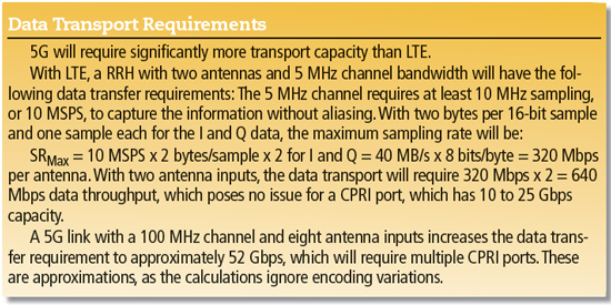
This article is intended to familiarize radio engineers with the use of a multi-purpose commercial off-the-shelf (COTS) platform for software-defined radio (SDR) that can reduce development time for 5G.
COTS SDR has been traditionally used in military radar and communications applications for high performance and design flexibility. The latest COTS SDR products offer solutions with integrated I/O, ARM processors and large FPGAs that also include intellectual property (IP) for accessing, routing and processing digital data. These attributes, combined with superior signal integrity, phase-coherent sampling and multi-channel transceivers, make a COTS SDR system an ideal choice for a 5G development platform.
COTS SDR DEFINED
For clarity, each section of this article is divided into subsections discussing hardware, firmware and software. Hardware comprises the SDR printed circuit board (PCB) and supporting components; firmware includes the internal FPGA code for logic and digital signal processing (DSP) functions; and software is the C code that controls the FPGA with firmware and performs any additional DSP functions.
Hardware
An SDR replaces legacy analog systems consisting of RF filters, analog down-convertors (i.e., the local oscillator and mixer), bandpass filters and demodulators (see Figure 1a). These fixed analog systems are limited to a specific function, such as an AM or FM radio.
An SDR exploits programmable DSP techniques to flexibly handle the increasing complexity, precision and bandwidth of today’s radio traffic. To use the SDR, data conversion is required between the antenna and DSP for both receive and transmit functions.1 An SDR receiver converts an RF signal from an antenna into digital samples with an analog-to-digital converter (ADC) and uses subsequent DSP operations to extract the required information from the signal (see Figure 1b). An SDR transmitter accepts digital information to be transmitted and performs the necessary DSP operations to produce digital samples for a digital-to-analog converter (DAC), whose output drives a power amplifier for delivery to the antenna (see Figure 1c). Because these radios are software-defined, they can be programmed on-the-fly in microseconds with new parameters or re-configured for different purposes by simply loading new firmware from internal or external memory.
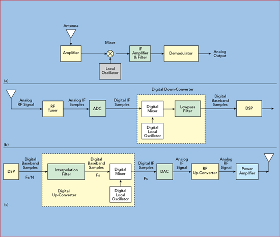
Figure 1 Legacy analog communications receiver (a) vs. SDR receiver (b) and SDR transmitter (c).
An SDR is often implemented on a specialized PCB called a “mezzanine card.” The current generation is either a switched-fabric mezzanine card (XMC) or an FPGA mezzanine card (FMC). Figure 2 shows XMC and FMC mezzanine cards with their corresponding functional block diagrams. Figure 2a is an XMC card with four 200 MHz ADC channels, and Figure 2b is an FMC card with two 3 GHz ADC channels and two 2.8 GHz DAC channels. Each board includes a precision timing system with a multi-bit, fractional synthesizer for variable sampling rates, which is locked to an on-board oven-controlled crystal oscillator (OCXO) or a reference input signal. These timing systems usually accept external synchronization signals from a network time protocol server or GPS receiver for the precise timing requirements of a radar or cellular system. Precise time alignment is also required for phase-coherent sampling of the ADCs, FPGA DSP data synchronization and DAC signal transmission.
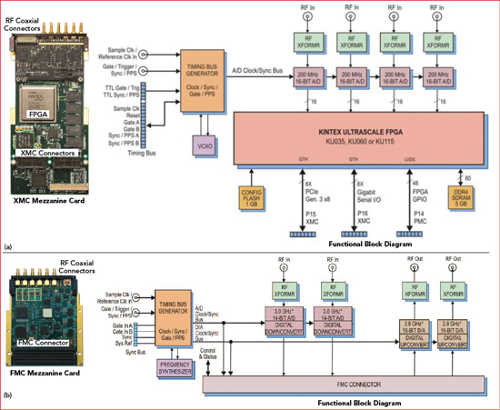
Figure 2 XMC (a) and FMC (b) mezzanine cards and functional block diagrams.
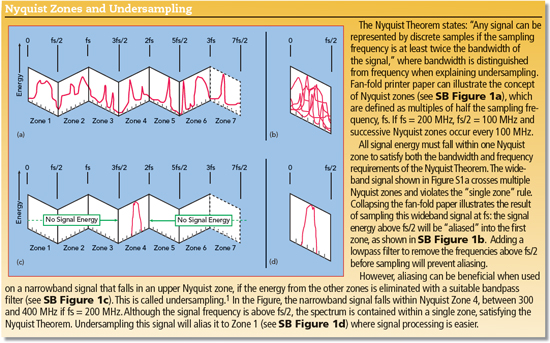
The XMC ADC has a 200 MSPS maximum sampling rate that can capture a 100 MHz Nyquist bandwidth, excluding filtering. A common technique with digital radio is to acquire channel information or intermediate frequency (IF) bandwidth by undersampling the signal (see Sidebar Nyquist Zones and Undersampling). Undersampling allows an ADC with a lower sample rate and higher dynamic range to capture a narrow bandwidth signal centered at a higher frequency without loss of information. For this to work correctly, the RF input path and the ADC must accommodate these higher frequency signals.
After analog-to-digital sampling, the next stage is typically the digital down-convertor (DDC), which performs frequency translation and bandwidth reduction. The DDC is often implemented as IP firmware within the FPGA.
Firmware
An FPGA consists of unconnected logic, arithmetic and signal processing building blocks that are configured with IP firmware to perform specific functions. While ideal for extreme programming flexibility, firmware development is complex. To simplify the development process, some COTS SDR manufacturers provide FPGA IP for basic operation of their boards. This usually includes analog and digital I/O functions for acquiring and transmitting data, with DSP IP for specific radio functions like DDCs, filters, channelizers and engines to transfer data to the system.
The DDC function requires three IP building blocks: the numerically controlled oscillator (NCO) local oscillator, a complex mixer and digital filters to replace the functions of the legacy analog radio system (see Figure 1). The tuning stage of the DDC uses a complex digital mixer to translate the frequency of interest to baseband. A pair of multipliers driven by a direct digital synthesizer (DDS) NCO allows the user to “tune” the receiver to the desired frequency. The samples are then passed through a lowpass finite impulse response (FIR) filter to decimate the signal for a finite channel bandwidth. Two key benefits of the DDC are higher signal-to-noise ratio (SNR), as a result of decimation, and the ability to tune to the narrowband center frequency of the signal (see Sidebar Improving SNR with Digital Processing). Decimating the signal effectively lowers the sample rate and reduces uncorrelated white noise, and the NCO enables precise digital tuning to a specific carrier frequency within a single Nyquist zone.
Software
While the vendor-provided FPGA IP might meet the specifications for a specific application, the system implementation may require controlling software to operate the radio. The FPGA IP needs operational parameters sent across the system interface from a software program, which is the function of a board support package (BSP) normally written as “C” callable routines for a Windows or Linux environment. The BSP contains library functions and pre-compiled example code that can be executed to test board functionality. One such function is commanding the ADC to capture and transfer data to the FPGA for further processing in the DDC. This processed data can be stored in memory or transferred to the DAC for conversion back to an analog signal and output for transmission. This is an example of a software program developed using the BSP software library functions and drivers. If any new FPGA IP is created by the user, additional control software must be written and included in the BSP package.