
A low cost printed planar filter on alumina ceramic substrate was developed at 60 GHz. This filter is advantageous in cost, size, weight and connectivity to MMICs. It is especially suitable for millimeter-wave module integration, where MMICs and filters are all assembled inside one compact package. The filter is based on a new equivalent circuit structure, which has two or four transmission zeros on both sides of the passband. The new feature of the structure is a mutual inductive coupling between the input and output ports. The equivalent circuit simulation exhibits more idealistic rectangle-shaped bandpass performance than a conventional bandpass filter (BPF) with two transmission zeros. The equivalent circuit is very simple, and easily fabricated in various styles, for operation at both millimeter-wave and microwave frequency ranges.
Recently, a millimeter-wave application for the home consumer market was proposed.1,2 In order that millimeter-wave technology may succeed in such a market, cost and size must be reduced drastically. Conventional metallic waveguide components are unacceptable. For such a market, the best solution for active components is MMIC technology. However, it seems that the best solution for passive components still remains unclear.
Among millimeter-wave passive components, designers are especially interested in filters because they are the component most difficult to planarize and can be a bottleneck for reducing the cost and size of millimeter-wave equipments.
INTEGRATED MILLIMETER-WAVE MODULE CONCEPT
In Japan, the development of integrated millimeter-wave modules has become intensive.3 The basic concepts of these developments are common. The module has two interfaces through its wall: one is a low frequency IF interface (pin, or SMA connector); the other is a millimeter-wave RF interface (antenna, V connector, or WR-15 waveguide). The users can utilize these modules as "black boxes." They simply connect an IF cable to these modules and obtain a millimeter-wave output, without requiring knowledge or skill in millimeter-wave circuit and assembly.
Figure 1 shows the aforementioned module concept, which the authors are developing.4 An MMIC mixer, an MMIC local oscillator and an MMIC amplifier are integrated inside a hermetically sealed compact ceramic package. On the backside of the package substrate, large scale array antennas are integrated. A slot type electromagnetic coupling connects the circuits on the upper side and antennas on the backside through the multi-layered ceramic substrate.
|
|
|
|


Note that the BPF (to reject the image, and, if possible, the local frequencies) must be located between the MMIC mixer and the MMIC amplifier. Therefore, it is necessary to integrate both filters and MMICs inside one small package. Balance mixer technology or anti-parallel diode pair (APDP) mixer technology can help reject the image or local frequency; however, it seems that the bandwidth and rejection values of those technologies are still limited. System design without any RF filters still seems unrealistic. For this reason, size, cost and connectivity (to MMICs) of millimeter-wave filters are critical problems.
In general, the most distinct requirement for millimeter-wave filters is the steepness between pass and rejection bands. For example, many system designs require a 1 GHz IF signal directly up-converted by a 60 GHz local frequency. As a result, the RF band, image band and local frequency are located very close to each other. This is the reason why conventional metallic waveguide filters are still widely used. Simple planar type filters were believed to be unable to meet the steepness requirement.
Some researchers have proposed semi-planar filter structures to improve steepness.5,6,7 The common concepts suggested are to take quasi three-dimensional structures to shield radiation, reduce transmission loss and improve the Q of the resonators. Their approaches can be summarized as hybrid solutions of planar structure and metallic waveguide structures. However, these quasi three-dimensional structures are not suitable for the module concept proposed.
Another complication related to steepness is bandwidth. In general, extremely wide bandwidth is an important factor when the frequency goes up higher into the mm-wave region. The applications previously published1,2 also require 1 to 3 GHz bandwidth. However, usually steepness and bandwidth of filters are opposite trade-off requirements. The recent trend of wider bandwidth makes planar type millimeter-wave filters more disadvantageous.
The approach taken here is different from those described previously.5,6,7 Because the module concept proposed is based on ceramic substrate a simple microstrip line type planar filter is chosen, printed and co-fired on the same ceramic substrate. However, a new filter equivalent circuit structure is developed.
CIRCUIT DESIGN
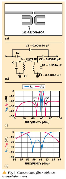
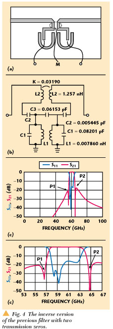
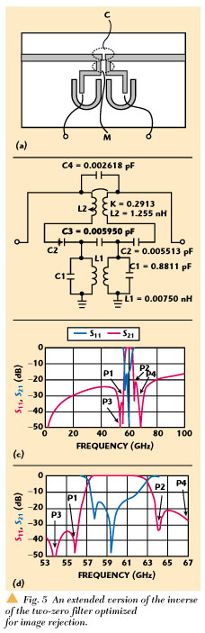
Figure 2 and Figure 3 show conventional filters, and Figure 4 and Figure 5 show the new developed filters. In each illustration, figure (a) depicts the basic layout, figure (b) depicts the equivalent circuit, and figures (c) and (d) depict the equivalent circuit simulation results in wide span and narrow span graphs, respectively. All of the filters compared here have only two λ/2-resonators because a reduction of the number of λ/2-resonators helps reduce insertion loss and layout size.
|
|
|
The first filter is shown the most basic conventional bandpass filter, with no transmission zero. The second filter is the most basic conventional filter, with two transmission zeros (P1, P2) on both sides of the passband.5 The two λ/2-resonators are coupled by mutual inductance, while the input and output ports are coupled by capacitance.
The third filter is the one proposed, with two transmission zeros (P1, P2) on both sides of the passband. The two λ/2-resonators are coupled by capacitance, while the input and output ports are coupled by mutual inductance. In this case, the filter structure can be regarded as an inverse version of the previous one. However, the numerical experiments shown below exhibit a steepness that is drastically improved over that of the previous one. In the new layout, in order to enhance the mutual inductive coupling M by maximizing the current, the coupling location is designed to be approximately λ/4 away from the microstrip line open ends O.
 In the methodology to compare performances of these filters, neither measurements nor electromagnetic simulation are relied upon. These comparison methods depend too much on how well the circuit layouts are optimized, and then the true potentials of circuits to be compared are often missed. The comparison methodology taken was the equivalent circuit simulation. The equivalent circuits are optimized by a commercial circuit simulator (Ansoft Corp., Serenade) under the same optimization goal conditions listed in Table 1.
The element values after circuit optimization are indicated, and simulation results are shown in the figures. Notice that difference in steepness between the different filter structures is remarkable. According to our equivalent circuit simulation, the two transmission zeros in the newly developed filters can be located much closer to the passband than those in the basic filters, without disturbing the 50 Ω match in the passband. We put only two λ/2-resonators into the circuit, yet the bandpass performance is relatively close to an idealistic rectangular-shape. Further improvement is expected with additional λ/2-resonators.
The filter shown in Figure 5 is an extended version of the previous one, optimized for image rejection. For the original circuit, there is only one transmission zero on each side of the passband, and a rejection band created by only one transmission zero is quite narrow. Then, in order to create more transmission zeros, additional coupling C (capacitance C4) is added between the input and output ports. In this case, four transmission zeros (P1, P2, P3, P4) are created, which leads to broad rejection bands.
MEASUREMENT
The extended version filter was measured. Its geometrical parameters were tuned on a commercial moment method simulator (Zeland Inc., IE3D). The substrate is a 0.15 mm thick alumina ceramic (εr = 8.9). The line/space design rule of thick film patterning was 50 µm all over the layout. The input and output port microstrip lines are 150 µm width and 1 mm length. Figure 6 is a photograph of the test sample. The total layout area is less than 1 mm * 1 mm, except for the probing pads.
|
|
|


 The test sample was measured with V-band coplanar probes under LRM calibration. The results are shown in Figure 7. Although the filter performance is somewhat distorted compared to simulation results, four transmission zeros are created successfully, which improve the steepness remarkably. In the passband, the insertion loss is 2.6 to 4.0 dB and the return loss is greater than 17 dB. The rejection performance is summarized in Table 2.
The layout size is very small, and further reduction is possible by photolithographic fine patterning technology. The possibility exists that the filter can be put directly on GaAs MMIC chips without increasing the total cost of the whole system.
FABRICATION EXAMPLES AT MICROWAVE FREQUENCY
The proposed filter equivalent circuit is very simple and can be directly translated into various fabrication styles at different frequencies. As an example, a coaxial dielectric resonator filter style of fabrication for microwave cellular phones is discussed below. The discussion in this section is based only on numerical simulations. Actual measurement experiments are now under way.
Figure 8 shows an example of a coaxial dielectric resonator filter, fabricated with chip coil type mutual inductance. This example is a straightforward fabrication of the originally proposed structure, but is not very cost-effective.
|
|
|
|
|
|


Figure 9 shows a simplified fabrication example, where the mutual inductance is realized by a pair of two parallel microstrip lines printed on the circuit board. This structure is analyzed by simulation. Figure 10 shows the model obtained from a commercial circuit simulator (Serenade). The substrate is 0.5 mm thick FR-4 (εr = 4.6), and the line and gap widths of the parallel microstrip lines are 0.5 mm. The element values after optimization are given, and the simulated response is shown in Figure 11.
Among the circuit parameters, notice that the parallel microstrip lines with only 2 to 3 mm length are effective enough to realize the proposed filter structure, even at 2 GHz. The cost of this filter is the same as for a conventional filter, and its layout size can be almost the same if the parallel microstrip lines are folded and hidden, for example, in the space under the dielectric resonators.
Besides a coaxial dielectric resonator filter, the proposed equivalent circuit can be translated into multi-layered dielectric filters. It is applicable to BPFs and duplexers.
CONCLUSION
A simple filter structure, with transmission zeros on both sides of the passband, is proposed. The equivalent circuit simulation results show that this structure has the potential to realize idealistic rectangular shaped bandpass performance.
The fabrication feasibility of this filter structure was confirmed at 60 GHz through measurements. A simple microstrip-line style planar filter on ceramic substrate was developed, which is suitable for low cost, highly integrated millimeter-wave module concept.
Using numerical simulation, the fabrication feasibility of this filter structure was shown at microwave frequencies. As an example, a coaxial dielectric resonator filter style of fabrication was discussed.
ACKNOWLEDGMENT
The material for this article was first presented at the European Microwave Conference held in Paris, October 2000. *
References
1. E. Suematsu, et al., "Digital and Analog Satellites/Millimeter-wave Transmission Link," IEEE MTT-S International Microwave Symposium Digest, Vol. 3, 1999, pp. 10471050.
2. K. Hamaguchi, et al., "A Wireless Video Home-link Using 60 GHz Band: A Concept of Developed System," Proceedings of European Microwave Conference, Vol. 1, 2000, pp. 293296.
3. Y. Hirachi, et al., "Status of Millimeter-wave MMICs and Their Applications in Japan," Proceedings of European Microwave Conference, Vol. 1, 2000, pp. 7982.
4. Y. Amano, et al., "Multi-layered Substrates for Wireless Communication Modules at 60 GHz," Proceedings of European Microwave Conference, Vol. 2, 1999, pp. 301304.
5. P. Blondy, et al., "Low Loss Micromachined Filters for Millimeter-wave Tele-communication Systems," IEEE MTT-S International Microwave Symposium Digest, Vol. 3, 1998, pp. 11811184.
6. T. Hiratsuka, et al., "A Ka-band Diplexer Using Planar TE Mode Dielectric Resonators with Plastic Package," Proceedings of European Microwave Conference, Vol. 3, 1999, pp. 99102.
7. K. Takahashi, et al., "K-band Receiver Front-end IC Integrating Micromachined Filter and Flip-chip Assembled Active Devices," Proceedings of MTT-S International Microwave Symposium, Vol. 1, 1999, pp. 229232.
Yoshihisa Amano received his BS degree from Kyoto University, Japan. In 1998 he joined Sharp Corp., Japan, where he has been engaged in research and development on millimeter-wave filters and antennas.
Atsushi Yamada received his BS and MS degrees from Kyoto University, Japan. In 1991 he joined Sharp Corp., Japan, where he has been engaged in research and development on millimeter-wave mixer and multiplier MMICs, and antennas.
Eiji Suematsu received his BS and MS degrees in geology from Kumamoto University, Japan. In 1986 he joined Sharp Corp., Japan, where he has been engaged in research and development on LNA and millimeter-wave oscillator MMICs.
Hiroya Sato received his BS and MS degrees from Kyoto University, Japan. In 1985 he joined Sharp Corp., Japan, where he is now senior technical specialist in Advanced Technology Research Labs.