
An extraction procedure for thermal parameters of high power heterojunction bipolar transistors (HBT) with pulsed I-V measurements is presented. The pulsed measurements become essential to model thermal effect and frequency dispersion of high frequency devices. The measurement setup used here can be configured with commercially available components.
Accurate characterizations of active devices are the basic requirements for a successful circuit design. They have included I-V and S-parameter measurements at different biases when the most frequently used active devices for high frequency circuits are FETs, heterojunction FETs (HJFET) and HBTs. However, even basic I-V measurements pose some challenges. For example, GaAs FETs are known to suffer from low frequency dispersion, which means that I-V characteristics at high frequency are markedly different from their DC counterparts. Pseudomorphic HEMTs fabricated in some materials systems are fairly robust against this phenomenon, but it does exist to some extent. In HBTs, there is a systematic decrease in collector current under steady-state when internal power dissipation (Pdiss ) causes a rise in junction temperature.
Pulsed measurements allow more degrees of freedom in characterizing high frequency devices. They provide valuable insight into various aspects of the device as to which predominantly affects the observed characteristics. One of the features that the pulsed setup can provide is that the bias point, from which the I-V characteristics are measured by pulsing both the input and output terminal stimuli, can be set anywhere in the I-V plane. When the device is measured starting from different DC quiescent points with the same dissipated power, the data will contain the same thermal information illustrating how the trap effects are related to the bias point. Moreover, pulsed measurements with various pulse timing configurations will reveal temperature effect on the observed transient response.
PULSED MEASUREMENT SYSTEM
The measurement setup implemented to characterize trap and thermal effects is shown in Figure 1. The external equipment required to perform pulsed measurements is only a pulse generator. Both DC and pulsed I-V measurements can be performed by enabling or disabling the pulse generator. A digital oscilloscope may be configured to monitor voltage waveforms for possible oscillations, ringing or malfunctioning, but is not a necessity. Two multiplexers are used to switch to the pulsed bias and they are synchronized with the pulse generator. The resultant signals are amplified by current feedback type operational amplifiers and driver FET. The current driving capability is greatly enhanced here without sacrificing rapid transitions. The device under test (DUT) draws the output current from the driver FET, which should be selected carefully on the basis of maximum current capability and transient response.

There are generally two techniques to measure current under pulsed condition.1 The most widely used technique is to use a current probe and a sampling oscilloscope. The main drawback is that the measurement accuracy is limited by the conversion accuracy of the current probe and the resolution of the oscilloscope, which are generally not acceptable when accuracy is a matter of prime concern. In this setup, the voltage across a current sensing resistor (CSR) is monitored using sample and hold circuitry which is also synchronized with the pulse generator after an appropriate delay. Since high current devices often present an output resistance considerably lower than 1 Ω, it is better to locate the sensing resistor outside the signal path between the DUT and the driver FET. For voltage measurements, two sample and hold circuits are used. The resultant voltages are now compared to the specified reference voltages (VGP , VDP ) until the difference is minimized by a feedback mechanism that cannot be readily shown in the diagram. This is usually a difficult task under pulsed conditions. The offset error of sample and hold circuitry is a function of both the reference voltage and pulse width. However, the error is considerably lower under DC condition. Thus it is possible to compensate the offset by investigating the difference between two measured responses for a known standard such as a 50-Ω load in microwave calibration standard.
The implemented measurement setup presents a very low series resistance and inductance to the reference plane of the DUT since the driver circuit is in intimate contact with the DUT. The measurement module can be mounted on top of commercially available microwave probe tips. With this configuration, the setup can measure high power devices very accurately and reproducibly at high current density, and there is less chance to suffer from device oscillations, which could not be removed when commercial I-V measurement equipments were used. The sensing resistor for the gate terminal performs two functions: It adds damping to the input equivalent circuit of the DUT so that ringing and voltage spikes can be avoided; and the voltage drop across it is used to calculate the base current (IB )when the DUT is a junction-type device. When measuring HBTs, this resistor plays an important role. At this time, the voltage drop is fed back to compare it with a reference voltage whose value is the desired base current multiplied by the value of the sensing resistor. It was determined to be several hundred Ω considering the amount of damping necessary to prevent ringing and the maximum base current driving capability for most high power HBTs. An example of pulse shapes for 2 * 20 µm2 24 finger AlGaAs/GaAs HBT is shown in Figure 2. The rise and fall times were less than 30 ns in this case, showing no greater than 50 ns at full excursion. A summary of the current measurement setup is provided in Table 1.
|
|
|


The measurement speed can be increased when the setup is connected to a commercial parameter analyzer such as an HP4145 and 4156. They are equipped with two voltage source (VS) and voltage monitor (VM) units. Voltage source units can be used to generate reference voltages for the input and output terminals of the DUT, while voltage monitor units sample voltages across current sensing resistors. The resultant signals are displayed on the screen of the parameter analyzer graphically as in the conventional DC measurement case.
|
|


HBT THERMAL RESISTANCE MEASUREMENT
Negative differential resistance (NDR) can be observed in most HBTs under CW mode for collector current densities above ~104 A/cm2 . This is attributed to the decrease of the current gain (ß) according to the junction temperature rise caused by internal power dissipation. The most common approach to incorporate this phenomenon into a circuit simulator is to use a thermal subcircuit of the device. Thus it is very important to determine the thermal resistance (Rth ) and thermal capacitance (Cth ) accurately for a reliable circuit design.
There are mainly two electrical approaches for thermal resistance extraction. In a DC technique,2 temperature dependence of either current gain (ß) or base-emitter voltage (VBE ) is used to determine the thermal resistance. The DC method enables simple measurements, but it lacks accuracy because it doesn't exactly separate ambient temperature and power dissipation effects. Sometimes it leads to a rather unphysical conclusion that Rth decreases as the ambient temperature increases. In the pulse technique, two sets of measurements are required to determine the thermal resistance of the device. Isothermal or pulsed measurements should be performed in addition to non-isothermal or DC measurements. The pulsed method is inherently more accurate because under isothermal conditions, any junction temperature rise can be solely attributed to the ambient temperature (Tbase ) rise that is controlled by an external thermochuck. However, the previous technique3 doesn't reflect the true operation of HBTs because it stimulates the base with a constant voltage. To some extent, this technique can produce valid extraction results for devices with modest emitter size. As the device size increases, it is required to use a shorter pulse width to achieve isothermal conditions at the same current density level. Therefore it is better to use measurements under constant current because self-heating effects are less pronounced under constant current than constant voltage with the pulse width set to the lowest possible value. For modeling purposes, measurement data under both conditions are needed.
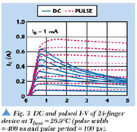
The DC and pulsed characteristics of a 24-finger device is shown in Figure 3. A pulse width of 400 ns with a period of 100 µs was used for the results presented in this article. The device is characterized by nearly ideal I-V curves under negligible internal power dissipation as can be seen in low collector current region of DC data and isothermal condition. But even in an isothermal measurement under pulsed conditions, the collector current (IC ) slightly decreases when Pdiss becomes too large. To avoid this problem, the width of the pulse signal should be narrower than the one configured here. However, these areas are usually not experienced in normal operation of an HBT because the collector current density is too high. In this work, five AlGaAs/GaAs HBTs with different emitter fingers (each of 24, 22, 20, 16 and 8 fingers) were investigated. All HBTs are assumed to have the same chip configuration except the number of emitter fingers.
At progressively higher current and temperature, IC is related to Rth , Pdiss and Tbase by2

where
T1 = temperature around which the linear approximation is made
ß1 = current gain at T1
In this equation, (Δß/ΔT) Rth can be extracted from the slope of the IC vs. Pdiss line at a constant Tbase , which was constructed from DC the I-V data, as shown in Figure 4. The slopes of the lines are measured to increase progressively as Tbase is increased. (Δß/ΔT) is extracted from isothermal measurement where Pdiss can be assumed to be zero. By using the setup presented here, the same IB condition as for the DC case is satisfied and the ß dependency on Pdiss can be effectively ruled out. It is important to ensure that all conditions are the same except Tbase so that the ratio between two curves produces Rth . (Δß/ΔT) was measured to be nearly linear and showed a negligible variance among different base currents, as shown in Figure 5.
Table 2 summarizes the measurement results at IB = 2.0 mA. The measured Rth for a 24-finger AlGaAs/GaAs HBT (2 * 20 µm2 /finger) ranges from 103.66 to 126.84°C/W as Tbase is varied from 26.9° to 71.7°C, and it seems to reflect the decrease of the thermal conductivity of GaAs according to the temperature increase. For comparison purposes, Rth was extracted using the same measurement data with the existing methods. The DC procedure of Dawson et al.2 produced Rth = 120.21°C/W at Tbase = 26.9°C and IB = 2.0 mA, which is in good agreement with our method. The pulsed procedure of McIntosh et al.3 produced 106.7°C/W for the same conditions. Based on this observation, it can be said that the pulsed method should be favored when accurate extraction is necessary. Figure 6 shows the extraction results of five HBTs at Tbase = 44.1°C. The values were fitted to a 1/x curve based on the fact that Rth scales inversely with total emitter area4 in a loose manner.
In the previously presented extraction procedure, DC measurement data were analyzed to obtain the current gain dependency on Pdiss . It is possible to get a similar result when pulsed measurement data are utilized. First, the device was measured under pulsed conditions starting from five different DC quiescent points with the same dissipated power (on the 600 mW-hyperbola), as shown in Figure 7. It is possible to say in this measurement that the device is relatively insensitive to trap conditions that are set by the quiescent point due to its vertical structure, and thermal effects play a more dominant role in output characteristics. The worst-case discrepancy between two measurement data in the active region was less than 3 percent. With DC quiescent points corresponding to progressively larger power dissipation, the same current gain decrease was observed, as shown in Figure 8. The slope which corresponds to (Δß/ΔT) Rth at Tbase = 26.9°C and IB = 2.0 mA was 56.960 [1/W], and this result is very similar to the value obtained from the previous DC measurement data.
|
|
|
|
|
|


THERMAL TIME CONSTANT MEASUREMENT
Pulsed measurements with different pulse widths can be used to extract the thermal time constant (*th ) of an HBT. As shown in Figure 9, the collector current decreases by a progressively larger amount as the pulse width increases from 400 ns to 10 µs, while the pulse period is maintained at 100 µs. The measured data were re-plotted as a function of pulse width for various collector to emitter voltage as shown in Figure 10, and it indicates that the collector current reduces rapidly within 2 µs and then slowly approaches a value corresponding to non-isothermal operation. Therefore, at least two time constants should be extracted to accurately model the measurement data in the form of Io (exp(t/*).5 The distributed thermal subcircuit can then be employed to describe the device characteristics. The extracted time constants were 6.39, 9.29 and 16.1 µs at VCE = 5, 4 and 3 V, respectively. Although the previous measurement results indicate an increase of Rth with Pdiss , the decreasing nature of *th with Pdiss is a clear sign that the thermal capacitance is also a function of dissipated power.
CONCLUSION
A procedure to extract thermal resistance and thermal time constant of an HBT with pulsed I-V measurements is demonstrated and compared to other approaches. The measurement results indicate that HBTs are relatively unaffected by traps. A pulsed measurement system for high current and high frequency devices has also been presented, which is compatible with commercially available components. This versatile setup provides a wide range of applications for device modeling.
ACKNOWLEDGMENT
The material for this article was first presented at the European Microwave Conference held in Paris, October 2000. *
References
1. B. Schaefer and M. Dunn, "Pulsed Measurements and Modeling for Electro-thermal Effects," BCTM Proceedings, 1996, pp. 110117.
2. D.E. Dawson, A.K. Gupta and M.L. Salib, "CW Measurement of HBT Thermal Resistance," IEEE Transactions on Electron Devices, Vol. 39, No. 10, October 1992, pp. 22352239.
3. P.M. McIntosh and C.M. Snowden, "Measurement of Heterojunction Bipolar Transistor Thermal Resistance Based on a Pulsed I-V System," Electronics Letters, Vol. 33, No. 1, January 1997, pp. 100101.
4. William Liu and Ayca Yuksel, "Measurement of Junction Temperature of an AlGaAs/GaAs Heterojunction Bipolar Transistor Operating at Large Power Densities," IEEE Transactions on Electron Devices, Vol. 42, No. 2, February 1995, pp. 358360.
5. Shawn S.H. Hsu, Donald Sawdai and Dimitris Pavlidis, "Modeling of Highly-nonlinear HBT Characteristics Using a Distributed Thermal Subcircuit Derived from Pulsed Measurements," 53rd IEEE Automatic RF Techniques Group (ARFTG) Conference, June 18, 1999.
|
|
 Hyun-Min Park received his BS and MS degrees in electrical engineering from the Korea Advanced Institute of Science and Technology (KAIST), Taejon, Korea, in 1997 and 1999, respectively. He is currently working toward his PhD degree at KAIST. His research interests include microwave power amplifiers, and active device modeling and characterization.
  Kye-Ik Jeon received his BS, MS and PhD degrees from KAIST (Korea Advanced Institute of Science and Technology) in 1991, 1993 and 1998, respectively, all in electrical engineering. From 1998 to 2000, he held the position of engineer at Material and Device Lab at the LG Corporate Institute of Technology (LGCIT), Seoul, Korea. During that time, he worked in development of various MMIC's and hybrid technology based circuits, including millimeter-wave power amplifiers, mixers, LNA and switches operating from L band through W band. His graduate research concerned the numerical charge control model of GaAs HEMT and MESFET. He also developed a 25 W feedforward multi-channel power amplifier for PCS application at KAIST in 1997. He operated Pulsed Measurements Inc., Seoul, Korea, from 1996 to 2000. He is now the president of RFcore Co. Ltd., Sungnam, Korea.
  Songcheol Hong received his BS and MS degrees in electronics from Seoul National University, Seoul, Korea, in 1982 and 1984, respectively. He received his PhD degree in electrical engineering from the University of Michigan, Ann Arbor, in 1989. Since March 1989, he has been a professor in the department of electrical engineering and computer science (EECS) at the Korea Advanced Institute of Science and Technology (KAIST), Taejon, Korea. His research interests include optoelectronic integrated circuits, quantum-effect devices and MMICs.