
Active millimeter-wave antennas will be deployed in unprecedented volumes over the next few years, fueled by the rapidly emerging 5G wireless (fixed wireless access and enhanced mobile broadband) and satellite communications systems. Millimeter-wave spectrum is attractive for telecom and satellite network operators due to the availability of large bands of contiguous spectrum, allowing for increased capacity, lower latency, and the ability to offer more services.
Unlike some of the early mmWave ICs used in military phased arrays, multi-channel silicon beamformer ICs are now recognized as being fundamental to reducing the cost of these active antennas as the way to commercialize phased arrays. The combination of high performance silicon processes together with advanced analog and digital design techniques has accelerated the adoption of mmWave ICs to the extent that advanced 5G and SATCOM networks are now anticipated several years earlier than the industry originally projected.
Additionally, there are several antenna system architectures being adopted for 5G, depending on fixed wireless access, traditional radio access networks, CPE and UE applications. In this paper, we will discuss some of the key considerations for active antennas for multiple applications and discuss how silicon ICs are addressing the needs to make the deployment of commercial phased arrays successful.
Active antennas, or phased arrays, have been widely used for many years. The first phased array applications were mainly military with systems deployed as early as the mid-1970s. Recent industry trends have shown a rapid increase in the use of this technology for both radar and communication systems, along with a push into the mmWave spectrum. This paper will explain the market changes behind these trends and the implications for the future.
Phased array technology offers some technical advantages, but also presents some special challenges, especially at the higher frequencies. Some of the basic figures of merit will be explained along with the key challenges. Industrialization will be one special challenge as the number of arrays climbs from thousands of units to multiple millions. Silicon technology with its proven reliability, high levels of integration, and low cost will be key to making this happen. All-silicon arrays will be the path forward for many radar and communications markets. Examples of some of these systems will be provided along with measured data.
Market Changes
The explosive growth of RF communication systems has made spectrum a scarce resource. The drive for more bandwidth has saturated the frequency bands from 700 MHz to 5.8 GHz. The only way to fuel the future demand for bandwidth is to push into the higher frequency bands – what we loosely term the mmWave range of 15-70 GHz. Many of these frequency bands are licensed by governments and reserved for satellite communications and military applications. Recently some of these bands have been opened for commercial communications to facilitate the emerging 5G standard. The US alone has now made available over 11 GHz of spectrum. Some key bands include 27.5-28.35 GHz, and 37-38.6 GHz in the US, and 24.25-27.5 GHz in Europe and China. Much of this is in flux as the scope of the 5G system is still being worked out. It is clear, however, that mm-Wave communications systems will become a commercial reality.
Satellite communications are also seeing significant growth. This is driven by the need for more bandwidth. Traditional satellite operators as well as some newcomers are scrambling to offer data services in the already licensed SATCOM bands. In parallel with this are some new proposed “Stratelite” systems. Instead of space based satellites, a network of balloons or drones can be created to produce a similar data communications system.
Another trend is being driven by advances in technology. The ability to create planar phased arrays that are much lighter than traditional systems is creating growth opportunities in the more traditional Aerospace and Defense market. Lighter and smaller arrays mean that radars can be deployed more easily and cost effectively and new applications are being developed to exploit this. In summary, three key markets – 5G, SATCOM, and A&D – are all driving a need for improved phased array technology.
Phased Array Technology
Active phased array antennas provide many advantages. Because they are steered electronically they can shift beam position very fast. Beams can commonly be made to sweep in several micro-seconds. The fact that there are no moving parts means that the overall reliability is much higher compared to a system that relies on physical movement such as a dish. Another reliability advantage is that if a single element fails the impact on the system is minimal. Thus there is a soft profile of degradation over the life of the antenna. Phased array technology is also scalable – by increasing the number of elements the radiated power can be increased and the system receive sensitivity is improved. This adds flexibility to the system design. Arrays that make use of high levels of integration to become planar arrays also have the benefits of being low profile and lightweight. The ability for the ICs to reside directly at the radiating elements minimizes feed loss which maximizes G/T and EIRP efficiency.
The emerging mm-Wave frequency bands have a high radiated path loss. This makes phased array technology ideal as multiple antenna elements can be located in a compact area to form highly directive beams. This directivity scales with the number of elements and can help compensate for the higher path loss. Use of multiple directive beams will enable spectral reuse increasing system capacity. Nulls can also be created and steered to reduce co-channel interference.
Even with all the advantages that phased arrays offer there are still unique challenges when implementing them at mmWave frequencies. Most importantly is the size of the antenna element spacing. Because this scales directly with free-space wavelength (typically λ/2), for a given number of elements in the array the size of an array at 40 GHz will be one quarter the size of one at 20 GHz. The challenge in creating a planar array at the higher frequencies is fitting the electronics within the lattice spacing as shown in Figure 1. This drives the integration level of the ICs. Fortunately, advances in silicon technology and design techniques have enabled products that are small enough to accommodate this tight lattice spacing. Integrated solutions are key, however, and these planar systems can no longer be made from discrete assemblies.
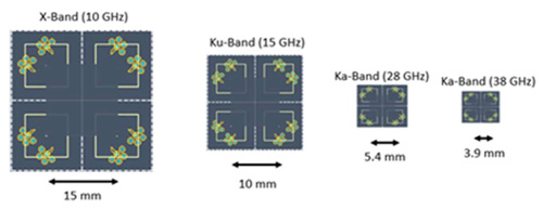
Figure 1. Size reduction of 4x4 array with frequency.
Another issue to manage is the thermal performance of the system. The radiated power required for a system at 40 GHz might be the same as one at 20 GHz but now the density of DC power that must be dissipated as heat has quadrupled. This makes the design of the heat sink and thermal management strategy for the system very challenging as shown in Figure 2. It also means that targeting high power levels per element will no longer be practical. A system-oriented strategy that employs more elements in the array to achieve the desired power is desirable. Because the Effective Isotropic Radiated Power (EIRP) scales with the square of the number of elements high power can be achieved with a modest increase in the size of the array.
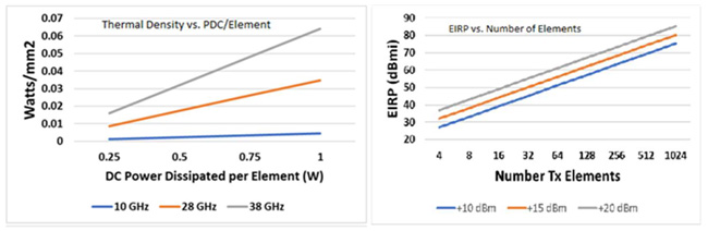
Figure 2. Thermal density vs. frequency, EIRP vs. number of elements.
The EIRP is an important figure of merit (FOM) for an antenna array. This is scalable with the array size and is proportional to N^2 where N is the number of elements in the array. Another, more difficult FOM to consider is the ratio of receiver antenna gain to receiver noise temperature, or G/T. This can be calculated at boresight as
G/T=4πAe/(λ^2*[Tsky+T_0 (NF*L-1)])
Where Ae is the effective radiating area, Tsky is the noise temperature of the sky, NF is the noise factor, L is the loss between the antenna and the receiver, and T0 is 290 deg-K. Unlike with EIRP, which scales as the square of the number of elements, G/T only scales directly with N. This puts an increased burden on the design of the receive chain. Another important thing to note is that the loss between the antenna and the LNA is critical and will degrade the receiver sensitivity directly.
The signal to noise ratio, SNR can be derived from Friis equation as:
SNR=Prx/No=EIRP/k*G/T*⌊λ/4πr⌋^2
Where r is the distance, and k is Boltzmann’s constant.
As an example, take an array with 64 elements at 28 GHz, lattice spacing of λ/2, Receiver Noise Figure of 4 dB, and loss to the element of 2 dB. If Tsky = 20 deg-K, the G/T can be calculated as -6.45 dB. It should be noted that a change to either noise figure or loss to the element impacts the SNR more than a 1:1 ratio depending on the relative values of the sky and receiver system temperatures. A 1 dB change, for instance, will degrade the SNR by 1.26 dB.
For phased array technology to realize the full growth potential offered by the promise of 5G and the SATCOM and A&D markets much will have to happen to make the systems low cost and reliable. Silicon is the best technology that can simultaneously achieve the high integration levels, low cost, and reliable performance to enable the volume phased array markets. Proof of concepts exists, what is left is continued work to commercialize the technology.
Figure 3 shows a block diagram for a commercially available beamforming IC at 28 GHz designed to fit behind 4 antenna elements in a planar phased array.
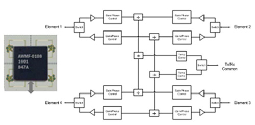
Figure 3. AWMF-0108 – 4 Element, 28GHz Beamforming IC.
A commercially available array made from the same beamforming ICs is shown in Figure 4. This is a 64 element rectangular array with LVDS, Ethernet, or USB digital interfaces. It offers an EIRP of greater than 50 dBmi, and a G/T of -6 dB/K. It runs off of a 12 V supply and consumes less than 20 W DC power.
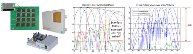
Figure 4. AWMF0129 – 64 Element, 28GHz Phase Array Antenna with beam steering data.
The array in figure 4 can be scaled to create larger arrays while also adding in flexibility. Figure 5 shows an array that scales the 64 element array into 4 sub-arrays. This can be configured to operate as 4 independent 64 element arrays or as 1 256 element array. Thus multiple data streams, MU-MIMO can be traded off for high power depending on the instantaneous power requirements for the system.
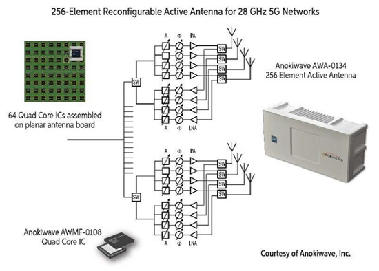
Figure 5. AWA-0134 – 4x64 Element array for MU-MIMO.
Conclusion
The path is clear for all-silicon arrays to be deployed in a variety of markets. The technology has moved beyond proof of concept and academic research. The required silicon components and full arrays are in production today. The years to come will see further productization as they move to high volume manufacturing. Cost reduction for the components will be straight forward. Real work remains to eliminate cost in the system with reduced calibration, and better thermal management. Additional features will also be introduced to take full advantage of the scalability of the phased array architecture.