
MEASUREMENT RESULTS AND DISCUSSION
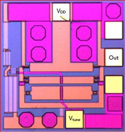
Figure 3 VCO die photo.
All of the passive components, such as the microstrip lines, capacitors and resistors are simulated with the Keysight Momentum electromagnetic simulator. Layout is accomplished using the Cadence Virtuoso layout suite based on transient and harmonic simulations of the design using ADS software. After rule checking and electromagnetic simulation, the designed VCO is fabricated in WIN 1 μm GaAs HBT technology. All devices are arranged symmetrically to have a differential output without the common node noise effect.
Figure 3 is a die photo of the entire circuit. The chip size is 0.65 mm × 0.68 mm including probe contacts. VCO performance is evaluated on wafer with a Cascade Microtech probe station. An HP4142B voltage and current source is used to supply the DC voltages ("VDD" and "Vtune"), meanwhile the output ("Out") is connected through a ground-signal-ground (GSG) probe with a 150 μm pitch width to a Keysight N9030A spectrum analyzer. With no differential measurement equipment available, the measurements are single-ended. The negative output is terminated with a 50 Ω load. The VCO is biased at VDD = 5 V (IDD = 10.2 mA ), consuming 51 mW of DC power.
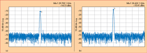
Figure 4 VCO output spectrum, Vtune = 0 V (a) and Vtune = 5 V (b).
Figures 4a and b show the VCO output spectrum with tune voltage Vtune of 0 and 5 V, respectively. The oscillation frequency variation as a function of control voltage sweep is plotted in Figure 5 from 29.71 to 30.43 GHz with control voltages between 0 and 5 V. The VCO exhibits a tuning range of 2.4 percent around a 30.07 GHz center frequency. A small (0.4 to 0.55 GHz) frequency discrepancy between simulated and measured results is due to parasitic effects of the layout. To improve simulation accuracy, software such as FastCap and FastHenry might be used for more precise simulation of the capacitors and inductors. In addition, some capacitance and inductance should be introduced in the simulation between the output and the termination load to account for parasitic effects produced by the contact between the probe and the tested chip.
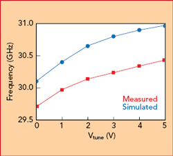
Figure 5 Simulated and measured VCO frequency vs. voltage.
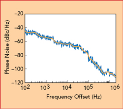
Figure 6 Measured VCO phase noise.
The phase noise of the VCO is difficult to measure, due to jitter caused by noise on the power supply and tuning voltages. The Keysight N9030A spectrum analyzer provides better phase noise accuracy at higher offset frequencies, so phase noise measurements are conducted from 100 Hz to 2 MHz offset (see Figure 6). The measured phase noise is −110.7 dBc/Hz at 1 MHz offset.
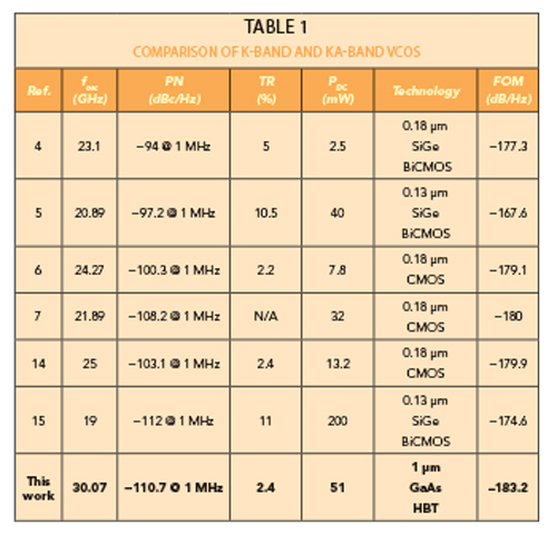
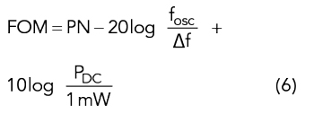
Table 1 compares the performance of this VCO with previously reported K- and Ka-Band VCOs. The commonly used FOM, which accounts for phase noise (PN), oscillation frequency (fosc), frequency offset (Δf) from fosc and power dissipation (PVCO),6 is used for comparison.
The VCO described in this article yields a lower FOM than others reported, demonstrating the capability of this design approach to achieve low phase noise performance at a high oscillation frequency.
CONCLUSION
A VCO employing a WIN 1 μm GaAs HBT and utilizing a fully differential Colpitts structure achieves low phase noise in Ka-Band. It demonstrates phase noise of −110.7 dBc/Hz at 30.07 GHz and 1 MHz frequency offset, with a DC power consumption of 51 mW from a single 5 V supply. Its FOM of −183.2 dB/Hz is better than others recently reported.
ACKNOWLEDGMENT
This project is supported by the National Basic Research Program of China (Grant No. 2010CB327505), the Advance Research project of China (Grant No. 51308xxxx06), the Doctoral Scientific Research Foundation of Henan University of Science and Technology (Grant No.400613480011), the Foundation of He’nan Educational Committee (Grant No. 15A510001, 14B510004) and the International Science and Technology Cooperation Program of Henan Province (Grant No. 144300510037).
References
- W. Simon, J. Kassner, O. Litschke, H. Fischer and S. Holzwarth, "Highly Integrated Ka-Band TX Front-End Module with an 8×8 Antenna Array," Microwave Journal, January 2011, Vol. 54, No. 1, pg. 58.
- C. S. Wu, H. C. Liu, H. C. Chiu and Y. F. Lin, "Ka-Band Bandpass Filter Using a CPW Structure Technology with Copper on an Al2O3 Substrate," Microwave Journal, June 2009, Vol. 52, No. 6, pg. 102.
- 3. S. W. Kang, J. C. Chien and A M Niknejad, "A W-Band Low Noise PLL with a Fundamental VCO in SiGe for Millimeter-Wave Applications," IEEE Transactions on Microwave Theory and Techniques, Vol. 62, No. 10, October 2014, pp. 2390-2404.
- Y. Huang Y, D. Wu, L. Zhou L, F. Jiang, J. Wu and Z. Jin, "A 23 GHz Low Power VCO in SiGe BiCMOS Technology," Chinese Journal of Semiconductors, Vol. 34, No. 4, April 2013, pp. 045003 –1-4.
- J. He, J. Li, D. Hou, Y. Z. Xiong, D. L. Yan, M. A. Arasu and M. Je, "A 20 GHz VCO for PLL Synthesizer in 0.13 μm BiCMOS," IEEE International Symposium on Radio-Frequency Integration Technology, November 2012, pp. 231–233.
- J. Yang, C. Y. Kim, Kim D. W. Kim and S. Hong, "Design of a 24 GHz CMOS VCO with an Asymmetric-Width Transformer," IEEE Transactions on Circuits and Systems–II: Express Briefs, Vol. 57, No. 3, March 2010, pp. 173–177.
- S. Wang and W. J. Lin, "A K-Band Gm Boosting Differential Colpitts VCO in 0.18 μm CMOS," Asia-Pacific Microwave Conference Proceedings, November 2013, pp. 1042–1045.
- S. P. Voinigescu, A. Tomkins, E. Dacquay E, P. Chevalier, J. Hasch, A. Chantre and B. Sautreuil, "A Study of SiGe HBT Signal Sources in the 220 to 330 GHz Range," IEEE Journal of Solid-State Circuits, Vol. 48, No. 9, September 2013, pp. 2011–2021.
- P. Andreani, X. Wang, L. Vandi and A. Fard, "A Study of Phase Noise in Colpitts and LC-Tank CMOS Oscillators," IEEE Journal of Solid-State Circuits, Vol. 40, No. 5, May 2005, pp. 1107–1118.
- J. Zhang, Y. Zhang, H. Lu, Y. Zhang and M. Liu, "A Novel Model for Implementation of Gamma Radiation Effects in GaAs HBTs," IEEE Transactions on Microwave Theory and Techniques, Vol. 60, No. 12, December 2012, pp. 3693–3698.
- T. K. Johansen and L. E. Larson, "Optimization of SiGe HBT VCOs for Wireless Applications," IEEE Radio Frequency Integrated Circuits Symposium, June 2003, pp. 273–276.
- J. C. Nallatamby, M. Prigent, M. Camiade and J. Obregon, "Phase Noise in Oscillators–Leeson Formula Revisited," IEEE Transactions on Microwave Theory and Techniques, Vol. 51, No. 4, April 2003, pp. 1386–1394.
- 13. T. O. Dickson and S. P. Voinigescu, "SiGe BiCMOS Topologies for Low-Voltage Millimeter-Wave Voltage Controlled Oscillators and Frequency Dividers," Topical Meeting on Silicon Monolithic Integrated Circuits in RF Systems, January 2006, pp. 273–276.
- T. Y. Lian, K. H. Chien and H. K. Chiou, "An Improved Gm-Boosted Technique for a K-Band Cascode Colpitts CMOS VCO," Asia-Pacific Microwave Conference Proceedings, November 2013, pp. 685–687.
- W. Wang, Y. Takeda, Y. S. Yeh and B. Floyd, "A 20 GHz VCO and Frequency Doubler for W-band FMCW Radar Applications," IEEE 14th Topical Meeting on Silicon Monolithic Integrated Circuits in RF Systems, January 2014, pp. 104–106.
Jincan Zhang received his M.S. degree at Xi’an University of Technology, China in 2010 and his Ph.D. degree in 2014. He is currently a lecturer at Henan University of Science and Technology, China. His research is focused on modeling of HBTs and design of very high speed integrated circuits.
Yuming Zhang received his M.S. and Ph.D. degrees in microelectronics engineering from Xidian University, China, and from Xi’an Jiaotong University in 1992 and 1998, respectively. From 1999 to 2000, he was with Rutgers University, N.J. as a postdoctoral fellow. Since 2001, he has been a professor at the Microelectronics Institute, Xidian University. His research field is in the design, modeling, fabrication and electrical characterization of SiC electronic devices for high temperature and high-power operation.
Hongliang Lu received her M.S. and Ph.D. degrees in microelectronics engineering from Xidian University, China in 2003 and 2007, respectively. Since 2010, she has been a professor in the School of Microelectronics, Xidian University. Her work involves the modeling and experiments on SiC MESFETs and other devices.
Yimen Zhang is a professor at the School of Microelectronics, Xidian University, China. He has been a visiting scholar and senior visiting scholar at Arizona State University, Tempe, and Yale University, Conn., respectively. His research interests are in the areas of wideband semiconductor devices, semiconductor devices modeling, TCAD for VLSI and quantum well devices.
Bo Liu received his B.E. and M.S. and D.E. degrees in electronic engineering from University of Kitakyushu, Japan in 2005, 2008 and 2012, respectively. Since 2012, he has been an associate professor at Henan University of Science and Technology. His research interests include VLSI layout design and process variation analysis for analog IC design for manufacturability (DFM).
Leiming Zhang received his M.S. degree in University of Electronic Science and Technology of China (UESTC), Chengdu in 2008. He is currently a lecturer at the Henan University of Science and Technology, China. His research is focused on device modeling of CMOS and the design of mixed signal integrated circuits.
Jinchan Wang received her Ph.D. at Southeast University, China in 2009. She is currently an associate professor at Henan University of Science and Technology, China. Her research is focused on semiconductor materials and devices.
Qing Hua received his M.S. degree at Harbin University of Science and Technology, China in 2009. He received his Ph.D. degree in University of Electronic Science and Technology of China in 2015. He is now a lecturer at Henan University of Science and Technology, China. His research is focused on power devices and power modules.