
A Ka-Band voltage controlled oscillator (VCO) using GaAs Heterojunction Bipolar Transistor (HBT) technology in a fully differential Colpitts configuration achieves low phase noise at a high oscillation frequency. It operates from 29.71 to 30.43 GHz and its phase noise is −110.7 dBc/Hz at 1 MHz offset at 30.07 GHz. It consumes 51 mW from a 5 V supply and occupies an area of just 0.65 mm × 0.68 mm. Its figure of merit (FOM) is −183.2 dB/Hz.
Ka-Band systems have many applications.1-2 Compared to Ku- and K-Band, the main advantages are a wider available bandwidth for faster communication and shorter wavelengths for higher radar/imaging resolution. In Ka-Band transceivers, VCOs are key components, with most systems requiring low LO noise (jitter) to minimize system errors. In particular, resolution and quality are degraded by high phase noise in imaging systems, and signal-to-noise ratio (SNR) improvement is hampered in beam forming systems. Data-acquisition rates can also be significantly reduced due to high jitter.3
At mmWave frequencies, two topologies, the cross-coupled VCO4-6 and the Colpitts VCO,3,7-8 are widely used. Andreani et al.9 have shown that both topologies are capable of very good phase noise; however, it is well known that the maximum oscillation frequency of a Colpitts VCO is higher than that of a cross-coupled VCO.3
The design of a fully differential Ka-Band Colpitts VCO is described in this article, which achieves low phase noise at a high oscillation frequency. At high frequencies, the differential VCO offers unique advantages over a single-ended configuration. These include a simplified front-end due to the directly fed differential LO inputs to the double balanced down-conversion mixers, substantially reduced on-chip noise generation and less sensitivity to supply voltage variations and noise.
The VCO is implemented in 1 μm GaAs HBT technology, which has a competitive performance advantage over other technologies. Compared with CMOS, GaAs HBTs offer potentially higher fT, higher transconductance and lower 1/f noise. In addition, GaAs HBTs have been shown to be inherently radiation hard, making them well suited for use in space.10
CIRCUIT DESIGN
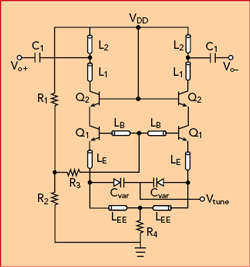
Figure 1 Differential Colpitts VCO schematic.
The technology used in this work is the GaAs HBT process from WIN Semiconductors Corp. The process offers four types of NPN transistors-Q1H051B1, Q1H101B1, Q1H151B1 and Q1H201B1-with different emitter lengths (5, 10, 15 and 20 μm, respectively). The main electrical features for these devices are the breakdown collector-emitter voltage BVCEO = 9 V, the maximum unit current gain frequency fT = 65 GHz and the maximum unit power gain frequency fmax = 80 GHz. Passive components, including two metal layers, two types of capacitors, resistors, varactor diodes, inductances and back side via holes are available in the process. Passive and active device models have been implemented and validated through simulation with Keysight Advanced Design System (ADS) software.
The VCO schematic, based on a differential Colpitts architecture, is shown in Figure 1. The inductor (LB) and the capacitors (Cvar and the base-emitter junction capacitor of the HBT CBE) form the resonating tank. The oscillation frequency is given by
To achieve a wide tuning range, Cvar is usually set to be far less than CBE,3 so that
To improve phase noise and design robustness, a number of developments borrowed from LNA designs are simultaneously applied:
1) A cascode buffer (Q2) is stacked on top of the VCO tank circuit such that they share the DC current to reduce overall current consumption. With this approach, additional buffers are not needed for tank isolation because of the cascode-style isolation of the tank.3
2) An emitter degeneration inductor LE is inserted to increase transistor linearity.
3) An inductor LEE is used to isolate the half circuits, thereby allowing for a single tail bias.
4) The current source is replaced with a resistor to minimize DC noise.11
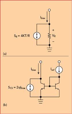
Figure 2 Circuit representation of resistor bias (a), current source (b).
It is easily demonstrated that resistor bias contributes less noise than a current source by first considering the spectral noise densities of the two bias circuits shown in Figure 2. For the spectral noise density of the resistor (SR) to be lower than the spectral noise density of the current source (SCS), Equation 3 must be satisfied.

VR, the voltage drop across the bias resistor, is typically greater than 150 mV to provide sufficient headroom for tuning the varactors.
DESIGN FOR LOW PHASE NOISE
The phase noise for a Colpitts oscillator is given by Equation 3,12 where Vtank is the voltage swing in the tank, In represents all noise sources of the HBT and Δω is the frequency offset from the carrier. It is apparent that Vtank must increase and In must be reduced to minimize oscillator phase noise.

Three effective ways to obtain high Vtank are by maximizing the bias current, by biasing at the peak fT/fmax current density of Q1 and by maximizing the Q of the resonating tank (Qtank). In addition, care must be taken not to exceed the breakdown voltage of Q1. The size of the transistors should be selected large enough to be able to apply high bias current; however, maximizing the bias current leads to high power consumption. There is always a compromise, therefore, between the high Vtank of an LC VCO and its power dissipation. Because this work focuses on absolute performance rather than low power consumption, the largest HBT (Q1H201B1), with a bias current of 9 mA, is used.
Q1 should be biased at the optimal noise figure current density (JNFMIN) that minimizes In. In the mmWave band, correlation between base and collector noise currents pushes JNFMIN close to the peak fT/fmax current density.13 Furthermore, biasing at the peak fT/fmax current density also increases Vtank. For these reasons, the optimum phase noise bias current density of the Ka-Band VCO shifts towards the peak fT/fmax current density.
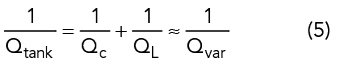
Qtank is another important parameter. It affects most VCO properties, including overall tank loss, power dissipation and phase noise. In lower frequency bands (< 10 GHz) the tank is dominated by the Q of the inductor (QL). However, as the frequency increases to above 30 GHz, the Q of the varactors (Qvar) decreases significantly.3 Thus, Qvar determines Qtank at the mmWave frequencies.
At the same time, the tuning range is also determined by varactor size. Thus, it is critical to obtain high-Q and large-ratio (Cmax/Cmin) varactors to achieve better VCO performance. There is a tradeoff, however, between Qvar and capacitance ratio.3 If a large capacitance ratio is chosen, the tuning range is maximized but Qvar is minimized, thereby degrading the phase noise.
In addition, the varactor should be carefully placed in the circuit to reduce parasitics. In this work, a varactor diode with a length of 20 μm and a width of 10 μm is chosen to balance Qvar and capacitance ratio.