
INVERTED DOHERTY
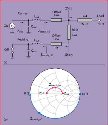
Figure 5 Load network (a) and impedance transformation (b).
Figure 4 shows the schematic of an inverted broadband Doherty amplifier with an impedance transformer using a quarter-wave line connected to the output of the peaking amplifier. This architecture can be helpful if, in the low-power region and depending upon the characteristics of the transistor, it is easier to provide a short circuit rather than an open circuit at the output of the peaking amplifier.9 In this case, a quarter-wave line is used to transform a very low output impedance after the offset line to a high impedance seen from the load junction. Taking into account the device package parasitics of the peaking amplifier, an optimized output matching circuit and a proper offset line can be designed to maximize the output power from the peaking device in the high-power region and approximate a short circuit in the low-power region.10
To better understand the operating principle of an inverted Doherty amplifier, consider the load network (see Figure 5a) when the peaking amplifier is turned off. In the low-power region, the phase adjustment of the offset line with electrical length θ causes the peaking amplifier to be short-circuited (ideally 0 Ω), and the matching circuit with offset line provides the required impedance transformation from 25 Ω to the high output impedance Zout seen by the carrier device output at 6 dB power back-off (ideally 100 Ω with the quarter-wave transformer), as shown in Figure 5b. In this case, the short circuit at the end of the quarter-wave line transforms to an open circuit at its input, preventing power leakage to the peaking path when the peaking transistor is turned off. In the high-power region, both carrier and peaking amplifiers are operating in parallel in a 50 Ω environment, and the output quarter-wave line with a characteristic impedance of 35.3 Ω transforms 25 Ω to the 50 Ω load.
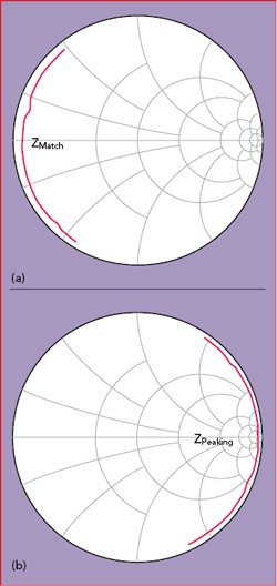
Figure 6 ZMatch (a) and ZPeaking (b) of the peaking amplifier from 1.8 to 2.7 GHz.
Using this configuration and two commercial 10 W GaN HEMT power transistors, the broadband inverted GaN HEMT Doherty amplifier was designed to achieve an average drain efficiency of 47 percent, average output power of 38 dBm (saturated power of 44 dBm) and a power gain of more than 11 dB across 1.8 to 2.7 GHz.7,11 The impedance at different points of the load network of the peaking amplifier when it is off are shown in Figure 6, where Zmatch (see Figure 6a) indicates low reactance at the output of the load network over the frequency range from 1.8 to 2.7 GHz, having near zero reactance at the mid-band frequency and some inductive and capacitive reactances when the operating frequency approaches the edges. By using a quarter-wave series transmission line, at higher frequencies an open circuit condition is provided with sufficiently high inductive and capacitive reactances across the band, indicated by Zpeaking in Figure 6b. Hence, the broadband performance of the inverted Doherty structure can be achieved in a practical realization.
Figure 7a shows the load network equivalent circuit for the carrier amplifier with the impedance Zcarrier seen by the carrier device, whose real component varies slightly around 10 Ω (see Figure 7b). Taking into account the device output shunt capacitance Cout of about 5 pF and series output inductance Lout provided by the bond wire and package lead frame inductances, the impedance seen by the device multi-harmonic current source across the frequency bandwidth of 1.8 to 2.7 GHz is increased by 2x from 5 Ω at the input of the broadband output impedance transformer, which is large enough to achieve high efficiency at back-off output power levels. In this case, the device output capacitance and bond wire inductor constitute a lowpass L-type matching section, increasing the load impedance seen internally by the device multi-harmonic current source at the fundamental frequency.
Figure 8 shows simulation results for the small-signal |S11| and |S21| versus frequency, demonstrating the bandwidth capability of a modified inverted transmission line GaN HEMT Doherty amplifier, covering 1.6 to 3 GHz with a power gain greater than 11 dB.
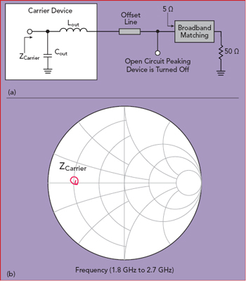
Figure 7 Matching network (a) and load impedance (b) for the carrier amplifier.
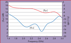
Figure 8 Simulated small-signal S-parameters vs. frequency.
TRI-BAND DOHERTY PERFORMANCE
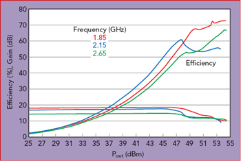
Figure 9 Simulated power gain and drain efficiency of the broadband inverted Doherty PA.
Figure 9 shows the simulated large-signal power gain and drain efficiency of a transmission line GaN HEMT tri-band inverted Doherty amplifier using a 20 mil RO4350 substrate, with the carrier gate bias Vgc = −2.5 V, peaking gate bias Vgp = −5.5 V and DC supply voltage VDD = 50 V. The design has an output power greater than 53 dBm and a linear power gain greater than 10 dB across the entire 1.8 to 2.7 GHz range. Drain efficiencies greater than 50 percent at saturation and 7 dB back-off are simulated at the center of the three bands-at 1.85, 2.15 and 2.65 GHz-with maximum drain efficiency greater than 70 percent at the lower frequencies and peak efficiency at maximum back-off output power of around 6 dB over the entire frequency range.
A test board of the tri-band inverted Doherty amplifier using two 80 W GaN HEMT power transistors with internal input matching and in metal-ceramic flange packages was fabricated on a 20 mil RO4350 substrate. The input splitter, a broadband Anaren model X3C17A1-03WS 90 degree hybrid coupler, has a maximum phase balance of ±5 degrees and amplitude balance of ±0.5 dB from 690 to 2700 MHz. The input matching circuit, output load network and gate and drain bias circuits (having bypass capacitors on their ends) were microstrip lines of different electrical lengths and characteristic impedances. The output lead inductances of the packaged GaN HEMT device were minimized.
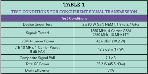
Figure 10 Measured performance of the broadband inverted Doherty PA.
Figure 10 shows the measured power gain and drain efficiency of the transmission line GaN HEMT inverted Doherty amplifier at five frequencies. A power gain greater than 9 dB was achieved from 1.8 to 2.7 GHz. Drain efficiencies greater than 55 percent at saturation (P3dB) and around 50 percent at 7 dB back-off were measured across the entire band, with the maximum drain efficiency greater than 70 percent at the frequencies below 1.95 GHz and peak efficiency points at maximum back-off power around 6 dB over the entire frequency range. The test conditions for concurrent transmission of a four carrier GSM signal and a 10 MHz LTE signal with a PAPR of 8 dB are shown in Table 1. A drain efficiency of 51 percent with an average total output power of 45.5 dBm (18.2 W for the GSM signal and 17 W for the LTE signal) were achieved using in-house digital predistortion (DPD) linearization. With dual-band DPD and the four carrier GSM signal, the out-of-band intermodulation levels were lower than −70 dBc. With the 10 MHz LTE signal, the adjacent channel leakage ratio (ACLR) was better than −57 dBc (see Figure 11).
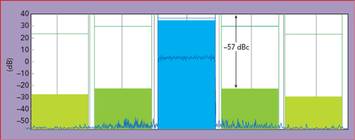
Figure 11 DPD linearization of the inverted Doherty amplifier with a 10 MHz LTE signal.
SUMMARY
To provide multi-band and multi-standard operation, LTE and 5G base stations are requiring that a power amplifier operate with high efficiencies over increasingly wide frequency ranges. Using GaN HEMT transistors and innovative Doherty architectures, tri-band coverage (1.8 to 2.7 GHz) with powers to 200 W and average efficiencies of 50 to 60 percent can be achieved, significantly reducing transmitter cost, size and power consumption.
References
- K. Bathich, A. Z. Markos and G. Boeck, “A Wideband GaN Doherty Amplifier with 35 Percent Fractional Bandwidth,” Proceedings of the 40th European Microwave Conference, October 2010, pp. 1006–1009.
- K. Bathich, D. Gruner and G. Boeck, “Analysis and Design of Dual-Band GaN HEMT Based Doherty Amplifier,” Proceedings of the 6th European Microwave Integrated Circuits Conference, October 2011, pp. 248–251.
- G. Sun and R. H. Jansen, “Broadband Doherty Power Amplifier via Real Frequency Technique,” IEEE Transactions on Microwave Theory and Techniques, Vol. 60, No. 1, January 2012, pp. 99–111.
- D. Y. Wu, J. Annes, M. Bokatius, P. Hart, E. Krvavac and G. Tucker, “A 350 W, 790 to 960 MHz Wideband LDMOS Doherty Amplifier Using a Modified Combining Scheme,” IEEE MTT-S International Microwave Symposium Digest, June 2014, pp. 1–4.
- N. Yoshimura, H. Umeta, N. Watanabe, H. Deguchi and N. Ui, “A 2.5-2.7 GHz Broadband 40 W GaN HEMT Doherty Amplifier with Higher than 45 Percent Drain Efficiency for Multi-Band Application,” IEEE Topical Conference on Power Amplifiers for Wireless and Radio Applications, January 2012, pp. 53–56.
- C. Monzon, “A Small Dual-Frequency Transformer in Two Sections,” IEEE Transactions on Microwave Theory and Techniques, Vol. 51, No. 4, April 2003, pp. 1157–1161.
- 7. A. Grebennikov, RF and Microwave Power Amplifier Design, 2nd edition, McGraw-Hill, 2015.
- D. Y. Wu, F. Mkadem and S. Boumaiza, “Design of Broadband and Highly Efficient 45 W GaN Power Amplifier via Simplified Real Frequency Technique,” IEEE MTT-S International Microwave Symposium Digest, May 2010, pp. 1090–1093.
- 9. L. F. Cygan, “A High Efficiency Linear Power Amplifier for Portable Communications Applications,” IEEE Compound Semiconductor Integrated Circuit Symposium Digest, October 2005, pp. 153–157.
- G. Ahn, M. Kim, H. Park, S. Jung, J. Van, H. Cho, S. Kwon, J. Jeong, K. Lim, J. Y. Kim, S. C. Song, C. Park and Y. Yang, “Design of a High-Efficiency and High-Power Inverted Doherty Amplifier,” IEEE Transactions on Microwave Theory and Techniques, Vol. 55, No. 6, June 2007, pp. 1105–1111.
- A. Grebennikov, “Multiband Doherty Amplifiers for Wireless Applications,” High Frequency Electronics, Vol. 13, May 2014, pp. 30–46.