

The 2019 defense budget seems to have something for everyone-including the first pay raise for troops in nine years-and sailed through the House with a 361 to 74 vote and was signed by the President. It is the first time in a decade this was achieved before the end of the fiscal year. By any unit of measure, 2019 should be a good year for the RF and microwave industry as the Defense Department's Third Offset Strategy requires a heavy dose of fields and waves.
Phased Array Radar
The U.S. has never faced the type and level of threats present today that require what only RF and microwave technology can deliver. For example, until recently, the U.S. and some NATO countries were the sole purveyors of active electronically-steered array (AESA) radars, but that is changing fast, as Russia and China have demonstrated their own formidable AESA systems. This is bad news for radar warning receivers (RWR) that are attempting to keep up with these shape-shifting electronic chameleons, whose lightning-fast reflexes and highly-developed brains can dispatch older RWRs with ease.
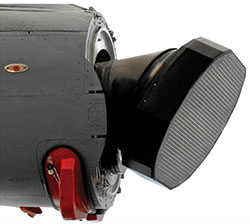
Figure 1 An AESA radar is smaller, lighter and vastly superior to legacy radars.
Even though phased-array radars have been in the inventories of the most advanced countries for a decade or more, the latest crop can exploit advances in signal processing to deliver astonishing performance. They can provide almost-instantaneous 360 degree coverage, and are versatile enough to perform in any role, from fire-control to synthetic aperture radar (SAR) mapping, sea surface search, ground moving target indication and tracking and air-to-air search and track. An AESA radar (see Figure 1) can randomly change frequency with every pulse, rapidly vary its output power, change its pulse repetition frequency and waveform, use spread-spectrum techniques and suddenly become passive, using the RWR's own signal to defeat it. And that is the short list.
AESA radars are also rapidly expanding their range, thanks in no small measure to GaN MMICs that are poised to complement or perhaps replace GaAs in the T/R modules of most next-generation radars, and many electronic warfare (EW) systems, as they too may use the AESA architecture. In fairness, without GaAs MMICs, the military might still be using traveling-wave tube (TWT) powered amplifiers for want of a broadband, solid-state alternative. GaAs is a mature, cost-effective technology whose future remains somewhat secure, if not in AESA radars, than in dozens of other applications that it has either enabled or enhanced.
The Triumph of the TWT
The imminent demise of the traveling-wave tube (TWT) has been predicted since the first GaAs MMICs led to the AESA radar and the last nail in the TWT's coffin was supposed to be GaN. Neither of these pronouncements has occurred and is not likely to for many years. In fact, the vacuum electron devices (VED) that helped win World War II and make SATCOM and radio and television broadcasting possible are experiencing resurgence with interest at mmWave frequencies, and DoD is a driving force.
No solid-state device can produce as much power in the mmWave frequencies and above than a TWT. However, the small size of solid-state devices allows phased-array antennas with hundreds of elements to produce a reasonable EIRP of perhaps 10 W at 60 GHz using a 64-element array. While this is more than adequate for commercial communications applications such as IEEE 802.11ad, more power is needed for EW systems. At higher frequencies above 100 GHz, the EIRP would be even less, and in all cases, heat dissipation is a major challenge.
The TWT that can deliver RF power of several hundred watts at frequencies up to 100 GHz and tens of W at 200 GHz, which makes it not only appealing but a necessity if EW systems are to defeat adversaries at these frequencies. Microwave Power Modules (MPM) that are even smaller at these high frequencies than their lower-frequency counterparts that potentially make them usable in airborne radar and imaging applications where SWaP requirements are severe. When fed to a high gain reflector-type antenna an EIRP of more than kW is achievable.
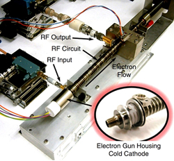
SB Figure 1 Anatomy of a 100 W cold-cathode TWT developed by L-3 Communications Electron Devices.
The power available from new TWTs may make them more enticing in the future, especially for remote sensing applications at higher frequencies. An example is a MPM designed by L-3 Electron Devices has an instantaneous bandwidth of more than 3 GHz from 231.5 to 235 GHz (G-Band) and produces a peak RF output power of 32 W with 10 mW of drive and efficiency of about 9 perccent (see SB Figure 1).
Cold Cathode Coming
The most noteworthy achievement in TWTs of late is the previously insurmountable challenge of producing a cold-cathode device, development of which has been ongoing since Charles “Capp” Spindt and Kenneth Shoulders of SRI International published a seminal paper in 1966. The benefits are significant, as a cold-cathode tube operates at ambient temperature without the need for a cathode heater, a traditional factor limiting tube life so that theoretically, tube life could be almost infinite. It would also eliminate warm-up time, making operation almost instantaneous. Current density could be much higher as well because emission would no longer be limited by operating temperature, making it easier to focus the electron beams.
The biggest challenge has always been reliability, as the cathode consists of tens of thousands of micrometer-size molybdenum cones deposited on a circular silicon substrate with an area of about one square millimeter. The high fields within the structure and the thin film gate electrode make it possible for an electrical short to occur between the gate and one of these cones. When that happens, the entire array of emitters burns up and the device fails catastrophically. In a traditional thermionic TWT degradation is “graceful,” allowing its end of life to be predicted by the amount of barium remaining.
However, L-3 Electron Devices has developed a way to reduce the damage caused by such a short, and were able to interrupt the breakdown path between the base of the cones and the gate by adding a dielectric layer between them. The company believes that at its current rate of development, the cold-cathode TWT could become a commercial product within about five years.
However, GaN has advantages that cannot be matched by GaAs, silicon or any other current semiconductor technology capable of producing RF power. It can operate at about 5× the voltage of GaAs and has 10× the power density per unit of die area, twice the current handling ability and higher power-added efficiency above about 10 GHz and higher than silicon above about 1 GHz. And while both GaAs and GaN can cover broad bandwidths, a GaN-based amplifier can have an instantaneous bandwidth 4× wider than a GaAs with the same output power.
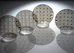
Figure 2 GaN on SiC wafers, shown here by the European Space Agency, have reached 6-in. in diameter.
Compared to silicon LDMOS, GaN has a power density advantage and can potentially operate far into the mmWave region. In short, GaN will power most of the radar systems and possibly EW systems in the future and has a long roadmap before it reaches maturity. LDMOS will continue to serve some radar as well as many communications applications for many years, at least for narrowband applications below about 4 GHz. LDMOS is the hands-down winner in terms of ruggedness and cost, with the ability to operate in a load mismatch or more than 65:1 while current commercial GaN on SiC devices (see Figure 2) are rated at 20:1 or less.
LDMOS discrete transistors can achieve high RF power levels, currently up to 1.8 kW with a bias voltage of 65 VDC as well. However, as LDMOS is a more narrowband technology so multiple amplifiers are required to cover a wide frequency range. LDMOS is still used in L-Band radar, IFF and avionics systems where it is competitive with GaN, and this market is highly competitive. GaN is also currently more expensive, but that may change as volumes increase.
Manufacturers of discrete GaN RF power transistors are actively pursuing the opportunities at L-Band with devices at various power levels. Qorvo's QPD1025 GaN on SiC transistor, for example, is currently the highest power, commercially available GaN on SiC device, delivering 1800 W from 1 to 1.1 GHz. Although narrowband, so are the key applications at L-Band that cover only 1030 to 1090 MHz. The device also operates at 65 VDC, directly targeting 65 VDC LDMOS with power-added efficiency up to 77 percent and gain up to 22.5 dB.
MACOM is a notable exception to the GaN on SiC trend as the company has dedicated its development efforts exclusively to GaN on silicon (Si) substrates and has a GaN on Si device that delivers 1 kW of pulsed power at L-Band. Although generally considered GaN's “second-tier,” MACOM believes it can make GaN on Si a formidable competitor for all but bleeding-edge (i.e., defense) applications. The primary advantage of silicon is its low-cost and proven high-volume manufacturability, as it can use standard CMOS fabrication processes, dramatically increasing product capability and reducing cost.
Current GaN devices have a power density of about 11 W/mm2 but several special processes have reported even higher levels. Fujitsu currently has the highest reported power density at 19.9 W/mm, although the DARPA GaN on diamond project reported results similar to this level a few years back. The ability to produce so much power from a tiny semiconductor device is remarkable and sure to increase in coming years. That is particularly appealing in an AESA radar where the ability to produce more power at each antenna element is highly desirable.
Advances in GaN's power density will result from enabling the technology to get as close as possible to its theoretical maximum. One of the ironies of GaN is that its enviable high-power density also results in the creation of heat in a very small area, so future achievements will be directly the result of getting rid of it, quickly as it is thermally limited in many cases.
This process begins at the die level, where silicon carbide (SiC), the material to which it is most often attached as a substrate, has thermal conductivity 6× that of GaAs and 3× that of silicon. Other material combinations such as copper-tungsten, copper molybdenum and copper-molybdenum-copper are used with silicon and GaAs devices, but currently only copper (and diamond in the future) can compete with SiC in thermal conductivity.
Once the heat is moved away from the die, the next stop for the heat is a structure that moves it further away, where it can be dissipated naturally or with liquid cooling. This can be a heat sink or heat spreader. The material that will allow GaN to achieve its potential is diamond as its thermal conductivity is 4× that of SiC or copper, in fact, higher than any other material on Earth.
There are some devices currently using diamond as a substrate material and aluminum-diamond metal-matrix composites (MMC) are used as heat spreaders. As applied to RF applications, chemical vapor deposition (CVD) diamond is the near-exclusive domain of Element Six (a subsidiary diamond goliath De Beers), which has achieved thermal conductivity of an astonishing 2200 W/mK. Their process for GaN on diamond devices was recently sold to RFHIC which plans to commercialize it. Nano Materials International (NMIC), which makes aluminum-diamond metal matrix composites used for heat spreaders, has achieved thermal conductivity of about 500 W/mK, and the composite is becoming more popular as GaN moves toward higher power densities. Akash Systems is using GaN on diamond exclusively to address satellite/space applications.
The DoD also wants GaN to operate at voltages higher than 50 VDC to increase efficiency and a few 65 VDC devices are available, including several from Integra Technologies, one of which operates between 420 and 450 MHz with a 150 VDC supply and delivers more than 1 kW with a 100 μs pulse width at a 10 percent duty cycle and drain efficiency greater than 70 percent. Several device manufacturers are offering these 65 VDC devices, such as Qorvo and Sumitomo, with others following.