
Fixed Wireless Access (FWA) has entered as one of the first enhanced mobile broadband (eMBB) use-cases. Many carriers are performing FWA deployment in targeted locations throughout their networks. In this technical paper, we analyze the architecture, semiconductor technology, and RF front-end (RFFE) design needed to deliver mmWave FWA services. Discussing topics such as;
- Scan-angle requirements
- Tradeoffs of Hybrid-beamforming versus All-Digital Beamforming for the Base Transceiver Station (BTS)
- Analyze BTS semiconductor technology and RF front-end components
- Gallium-Nitride on Silicon Carbide (GaN-on-SiC) front-end modules (FEMs) designed specifically for the 5G FWA
mmWave Spectrum & Deployment
Operators have already taken steps to meet their first FWA challenge: obtaining spectrum. Most deployments are expected to use mmWave frequencies, where large swaths of contiguous unpaired bandwidth are available at very low cost. Based on the initial trials and the geographical bandwidth it is clear the 26.5-29.5 GHz and 37-40 GHz bands will be the first used and 24.25-27.5 GHz will closely follow.
FWA describes a wireless connection between a centralized sectorized BTS and numerous fixed/nomadic users. Systems are being designed to leverage existing tower sites and support a low-cost self-installed CPE build-out. Both are critical to keeping initial deployment investment low, while the business case for FWA is validated.
Large coverage is essential to the success of the FWA business case. To illustrate this, let’s consider a suburban deployment with 800 homes/km2, as shown in Figure 1. For BTS inter-site distance (ISD) of 500 m, we need at least 20-sectors each covering 35-houses from 9 cell-sites. Assuming 33% of customers sign up for 1 Gbps service and a typical 5x network oversubscription ratio, an average aggregate BTS capacity of 3Gbps/sector is needed. This capacity is achieved in 800 MHz, assuming an average spectrum efficiency of 3 bps/Hz and 2-layers of spatial multiplexing. If customers are paying $100/month, the annual revenue is $280,000/km2/yr. Of course, without accounting for recurring costs it’s not clear FWA is a good business but we can conclude that as ISD increases the business-case improves. To that end, carriers are driving equipment vendors to build BTS and CPE equipment that operates up to regulatory limits to maximize coverage and profitability.
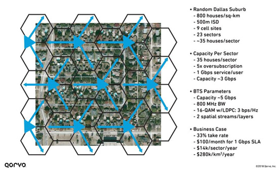
Figure 1. Fixed Wireless Access in a Suburban Macro Environment.
In the U.S., the Federal Communications Commission (FCC) has defined very high effective isotropic radiated base station power (EIRP) limits [1] at 75 dBm per 100 MHz for the 28 and 39 GHz bands. The challenge becomes building systems that meet these targets within the cost, size, weight, and power budgets expected by carriers.
FWA Link Budget
The standards community has been busy defining the performance requirements and evaluating several use-cases over a broad range of mmWave frequencies. The urban-macro scenario is the best representation of a typical FWA deployment; having large ISD of 300 to 500 m and providing large path-loss budgets that overcome many of the propagation challenges at mmWave frequencies.
Closing the link budget depends on many variables including transmit EIRP, receive antenna gain, receiver noise figure (NF), and minimum edge-of-coverage throughput. In the following, we explore several architecture trades that are key to technology selection and design of RFFE components.
Scan-Angle Requirements
The number of active channels in the array depends on many things. Let’s start by first understanding the scanning (azimuth and elevation) requirements and whether two-dimensional beamforming is required for typical FWA deployment or if a lower complexity one-dimensional (AZ only) beamforming array is sufficient. We will see that this decision impacts the power amplifier (PA).
We show two FWA deployment scenarios in Figure 2. In the suburban deployment, the tower heights ranging from 15 to 25 m and the cell-radius is 500 to 1000 m with an average house height of 10 m. Just as in traditional macro cellular systems, where the typically vertical beamwidth is 5-8 degrees, there is no need for fully adaptive elevation scanning.
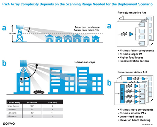
Figure 2. Array Complexity Depends on the Scanning Range Needed for the Deployment Scenario.
This allows the elevation beam-pattern to be focused down by corporately feeding several passive antenna elements, as shown in Figure 2(a). This vertically stacked column of radiating elements is designed to minimize radiation above the houses and fill in any nulls along the ground. Further, the gain pattern is designed to increase at relatively the same rate as the path loss. This provides a more uniform coverage for both near and far uses.
The nominal half-power beam-width can be approximated as 102°/NANT and the array gain by 10log10(NANT ) + 5 dBi. As we passively combine antennas the elevation beam pattern is focused, and fixed antenna gain increases, as shown in the Table of Figure 2. For the suburban FWA use-case, a 26° to 13° beam-width is sufficient and the passively combined column array can be 4 to 8-elements, respectively. In the urban scenario, the elevation scanning requirements are greater and systems will be limited to 1 or 2 passive elements. Figure 2 far right (a) and (b) illustrates the two approaches. Both have the same antenna gain but the column-fed array has a fixed elevation beam pattern. The per-element array supports wider scan angles but needs four times as many PA, phase shifter, and variable gain components. Whereas, the column-fed PA will need to be four times larger, which can easily change the semiconductor technology selection.
It’s reasonable to assume a suburban BTS will use antennas with 6 to 9 dB higher passive antenna gain compared to an urban deployment. As a result, the phased array needs far fewer active channels to achieve the same EIRP, significantly reducing active component count and integration complexity.
All-Digital and Hybrid Array Design
It is natural for BTS vendors to first explore extending current sub-6 GHz all-digital beamforming AAS platforms to mmWave. This preserves the basic architecture and the advanced signal processing/algorithms needed to realize beamformed spatial multiplexing. However, due to the dramatic increase in channel bandwidths offered by mmWave and the need for many active channels, there is a valid concern that the power dissipation and cost of such a system would be prohibitive. Therefore, vendors are exploring new hybrid-beamformed architectures [2], which allows flexibility between the number of baseband channels to the number of active RF channels. This approach may provide a better balance of analog beamforming gain and baseband processing. In the following sections, we analyze the two architectures and discuss the RFFE approaches needed for each.
All-Digital approach
The most obvious choice in mmWave base station applications is to upgrade the current platform. Three key elements would be required to do this, namely: efficient wide-band analog-to-digital/digital-to-analog converters (ADCs/DACs), highly integrated direct-conversion transceivers, and high-efficiency high-power amplifiers.
Analysis can show that even with todays off-the-shelf components and using a traditional high-power 9 W Psat linear GaN amplifiers (e.g. QPA2595) an all-digitally beamformed dual-polarized BTS can be designed to achieve 60 dBm EIRP/polarization with only 16 channels at a dissipated power of 320 Watts. Unfortunately, for all outdoor passive-cooled, tower-top electronics, it’s challenging to thermally manage more than 300 W from the RF subsystem. Fortunately, there are new technologies being introduced that will make this architecture a reality:
- Next-generation 14 nm digital-to-analog and analog-to-digital converters that save power
- Advances in mmWave CMOS direct-conversion transceivers
- Increased levels of small-signal integration
- Last but not least, new PA technology advances
As an example, Qorvo has been developing a 9 W Psat Doherty GaN PA at 28 GHz that provides over 20% PAE at 8 dB backoff. When compared to an equivalent traditional amplifier this is a 10% improvement and without any other changes to the above off-the-shelf design brings the dissipated power below 200 W. In combination with new ADC/DACs and highly integrated mmWave transceivers, the idea of extending a 16T16R Sub6GHz BTS platform to mmWave frequencies is nearer than most people think.
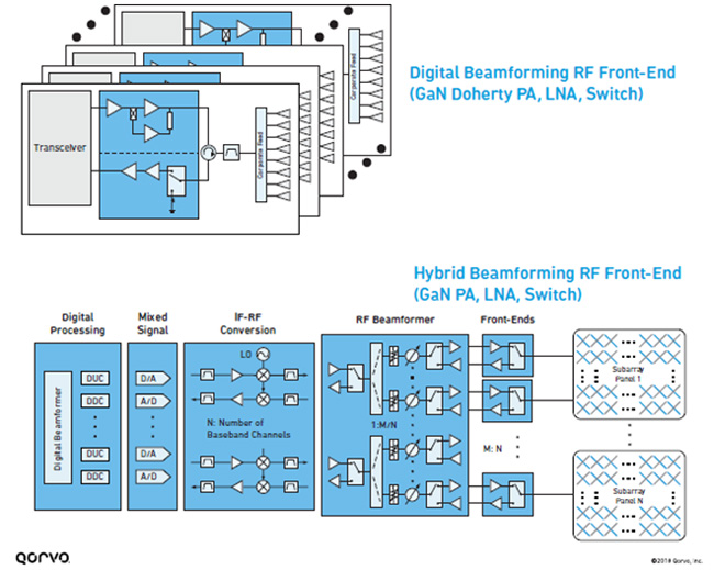
Figure 3. Digital and Hybrid RF Front-End Approaches.
Hybrid approach
An alternative architecture being explored is hybrid beamforming (Figure 3), where the spatial multiplexing and beamform precoding functions can be separated into digital baseband processing and analog RF processing, respectively. This provides a new design knob that allows the number of baseband chains to scale independently from the number of active antenna elements in the array. Unlike the all-digital architecture, where there is typically a 1:1 relationship with the number of active RF chains, the hybrid architecture allows a 1:N relationship.
As shown in Figure 3, the RF beamformer subsystem fans out the upconverted baseband stream into N branches, which are then adjusted for amplitude and phase, and fed to a multi-element panel antenna. By setting the correct phase and amplitude coefficients the radiated signals coherently combine to provide the needed beamforming gain in the direction of the intended user.
Although this approach reduces the number of ADC/DACs required, it sharply increases the number of RF front-ends that are needed and introduces the need for careful analog phase and amplitude control on each RF branch. Fortunately, these small-signal functions can be highly integrated on a single chip using SiGe semiconductor technology. The most typical configuration is to have 4-branches per core-beamformer chip but there are examples demonstrating up to 32-channels.
These core-beamformer chips act as a driver to feed the front-end modules (FEM) which provides the final PA, T/R switch, and LNA functions. If the required power from the FEMs is small enough, it is possible to also use SiGe technology and monolithically integrate into the core-beamformer chip. However, for base station applications where high EIRP is required, analysis shows that an all-SiGe solution will not provide optimum power consumption or cost because 1000’s of elements would be required. To optimize the cost and power consumption, it can be shown that using compound semiconductor technology, like GaN and GaAs, for the FEM allows the array size to be far less complex, consume less power, and be lower cost. The following section provides additional insight into this important trade.
Front-End Semiconductor Technology
The technology choice for the RFFE depends on the EIRP and G/NF requirements of the system. Both are a function of beamforming gain, which is a function of the array size. To illustrate this, we show in Figure 4(a), the average per-channel PA power (PAVE) needed as a function of array size and antenna gain for a uniform rectangular array achieving 65 dBm EIRP.
The graph is overlaid with an indication of power ranges that are best suited for each semiconductor technology. The limits were set based on benchmarks of each technology, trying to avoid exotic power-combining or methods that degrade component reliability or efficiency.
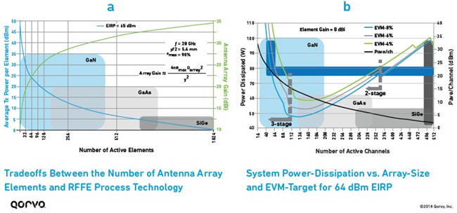
Figure 4. Technology System Trade-Offs.
As array size gets large (>512 active-elements) the power-per-element becomes small enough to allow SiGe/SOI, which could then be integrated into the core-beamformer RFIC. In contrast, by using GaN technology for the front-end, the same EIRP can be achieved with 8-to-16 times fewer channels. Now let’s examine these two cases further.
GaN versus SiGe Front-end Modules
System Power Dissipation
We start by analyzing the total system PDISS of the beamformer plus the front-end versus the number of active-array elements in each subarray-panel, as shown in Figure 4(b). The PDISS is shown for several error-vector-magnitude (EVM) levels and a requisite 64 dBm EIRP. EVM-level sets the back-off efficiency achieved by the front-end.
In this Figure 4b analysis, we assume that each beamformer branch consumes 190 mW. This is a typical power consumption of core-beamformers currently in the market [3]. The system on the far right (dark gray bar) represents an all-SiGe solution with 512-elements consuming ~100 W with an average power-per-element of 2 dBm. As we move left, the number of elements decreases, the PAVE per-channel increases, and we observe that PDISS is optimized up to a point where beamforming gain starts to roll-off sharply and PDISS needed to maintain the EIRP rapidly increases. The small steps in the dissipation curves represent the points where the front-end transitions from a single-stage, to 2-stage, and finally 3-stage design to provide sufficient gain. As stages are added the efficiency drops slightly and thus we see small jumps in power dissipation.
If we design to optimize system PDISS without regard for complexity/cost, an array of about 128-elements with a 2-stage 14 dBm (24 dBm P1dB) PA would make the best choice. However, if we strive to optimize cost/complexity/yield for a given budget of ≤100 W then the optimum selection (shown as the dark blue bar) would be 48-to-64 active channels using a 3- stage GaN PA with an average power of 20-to-23 dBm, depending on the EVM-target.
The trends shown in Figure 4(b) are less a function of PA efficiency and more a function of beamformer inefficiency. In other words, the choice to increase array size 8-fold to allow an all-SiGe solution comes with a penalty given that the input signal gets divided many more ways and requires power-hungry linearly biased devices to gain it back up.
Cost Analysis
The cost of phased-array systems includes the RF components, the PCB material, and the antennas themselves. Using compound-semi front-ends allows an immediate 8x reduction in array size with no increase to PDISS. Even with lower-cost printed antenna technology, this is a large saving in expensive antenna quality substrate material. But what about component cost?
Currently, the die cost per square-millimeter of 150 nm GaN-on-SiC on 4”-wafers is only 4.5-times the cost of 8” 130 nm SiGe. As we shift into high-volume on the 6”-GaN production lines, the cost relative to SiGe, drops to 3X. Using this information, we compare the relative raw die cost of the two systems based on the assumptions defined in Table 1 (a) and (b). The resulting cost comparison is summarized in Table 1(c).
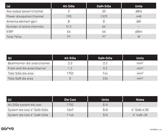
Table 1. Assumptions, Total Die Area, and Relative Cost of All-SiGe vs. SiGe Beamforming + GaN FEM Architecture.
We observe that using a high-power density compound-semiconductor solution like GaN on 6”-wafers can save up to 35% in raw die cost relative to an all-SiGe architecture. Put simply, even though the cost of silicon technologies is lower per device, the cost of the complete system is significantly higher. The savings in cost increased further when factors such as antenna substrate, packaging cost, testing time, and yield are considered.
A GaN FWA front end provides other benefits:
- Lower total power dissipation. GaN provides a lower total power dissipation than SiGe. This is better for tower- mounted system designs.
- Better reliability. GaN is more reliable than SiGe, with >107 hours MTTF at 200°C junction temperature. SiGe’s junction temperature limit is around 130°C. This has a big impact on the heat-sink design.
- Reduced size and complexity. GaN’s high power capabilities reduces array elements and size, which simplifies assembly and reduces overall system size.
Based on these trades, Qorvo has created a family of front-end modules for mmWave. These integrated modules include a multi-stage high-power PA, high linearity T/R switch, and low noise figure LNA, all monolithically integrated using our 150 nm GaN/SiC process.
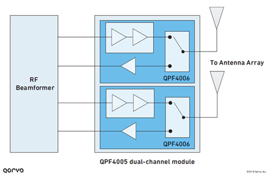
Figure 6. Qorvo FWA solutions: mmWave GaN front ends.
In addition to the above listed 39 GHz GaN components Qorvo also has similar modules addressing the 28 GHz market.Summary
FWA is rapidly approaching commercialization. Due in part to the abundance of low cost spectrum, early regulatory and standards work, and the opportunity for operators to quickly tap a new market. The remaining challenge is the availability of equipment capable of closing the link at a reasonable cost. Both hybrid-beamforming and all-digital beamforming architectures are being explored and analyzed. These architectures capitalize on the respective strengths and differences of semiconductor processes. The use of GaN front-ends in either approach provides operators and manufacturers a pathway to achieving high EIRP targets while minimizing cost, complexity, size, and power dissipation.
References
- Federal Communications Commission. (2016, July). Use of Spectrum Bands Above 24 GHz for Mobile Radio Services, In the matter of GN Docket No. 14-177, IB Docket No. 15-256, RM-11664, WT Docket No. 10-112, IB Docket No. 97-95. Retrieved from https://apps.fcc.gov/edocs_public/attachmatch/FCC-16-89A1.pdf
- A. F. Molisch et al., "Hybrid Beamforming for Massive MIMO: A Survey," in IEEE Communications Magazine, vol. 55, no. 9, pp. 134-141, 2017.
- B. Sadhu et al., "7.2 A 28GHz 32-element phased-array transceiver IC with concurrent dual polarized beams and 1.4 degree beam-steering resolution for 5G communication," 2017 IEEE International Solid-State Circuits Conference (ISSCC), San Francisco, CA, 2017, pp. 128-129.