
Part II of this bandpass filter tutorial features several examples that illustrate the general design procedure for bandpass filters using resonators and coupling methods of different types.
BANDPASS FILTER DESIGN
The general bandpass filter design procedure utilizes the normalized, low pass elements of the prototype filter to determine the required resonator coupling and coupling to the external circuit, that is, the source and load. In each case, the external source and load are assumed to be 50 Ω, although the filter could be matched to other real impedances.
The general design procedure is listed in Table 1. To illustrate the general bandpass filter design procedure, several examples are offered. It should be mentioned that the coupling parameters, that is, the capacitor matrix, or even and odd mode impedances, for several types of distributed resonators, may be determined with the aid of an electromagnetic (EM) simulator. This is an extremely valuable design tool because it eliminates the fabrication of models in order to determine the coupling of symmetrical, distributed resonators.

The illustrated examples include a lumped element, Chebishev, bandpass filter using π-type resonators, a coaxial cavity bandpass filter using  /8 resonators with capacitive tuning (comb-line), a coaxial cavity bandpass filter using /4 resonators (interdigital) and a half wavelength via-hole direct-coupled filter. Also described are a dielectric resonator, a bandpass filter using disk-shaped resonators, an inductively coupled filter in coplanar waveguide and a stripline or microstrip, Chebishev, bandpass filter using /2, side-coupled resonators.
Lumped Element Bandpass Filter
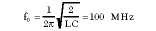
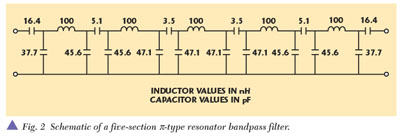
The lumped element, π-type resonator is used in a five-section, 0.01 dB ripple, Chebishev filter. The low pass prototype elements (g-values) may be calculated using the equations within the appendix or may be determined from available tabular data.
The filter parameters are
f0 = 100 MHz
Δf = 5 MHz
n = 5
rdB = 0.01 dB
g0 = g6 = 1.0000
g1 = 0.7563
g2 = 1.3049
g3 = 1.5773
g4 = 1.3049
g5 = 0.7563
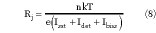
The unloaded quality factor for this type of resonator at this frequency is Qu = 250. A schematic of the resonator is shown in Figure 1.

BANDPASS FILTER DESIGN PROCEDURE
The bandpass filter design procedure is listed in Table 1. The values of the inductance and capacitors may be determined using
where

and

The inductance formula provides a good estimate of a convenient value of the resonator self-inductance from which the resonator capacitance may be calculated.
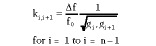
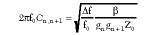
Next, the coupling values are calculated using
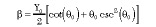
and the susceptance slope parameter is calculated as
ß = 1(2πf0 )C = 0.063662 mhos
The resonator coupling elements are determined using

and the input and output coupling are calculated as

and
The input and output coupling methods need not be the same as the resonator coupling. However, the input and output coupling must satisfy the relationship

and
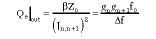
Table 2 lists the π-type resonator, bandpass filter data.

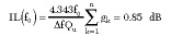
A schematic for the five-section, π-type resonator bandpass filter is shown in Figure 2. A computer simulation was conducted on the five-resonator bandpass filter using only the inductors as variable or tuning elements. The results of the simulation are shown in Figure 3. Note that the bandwidth is 5.12 MHz as compared to the design bandwidth of 5.0 MHz, and that the midband insertion loss is approximately 2 dB. The midband insertion loss of a bandpass filter may be estimated from the equation

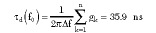
The computer simulation of the transmission group delay is also presented in the results. The midband group delay may be estimated from the formula
It should be mentioned that the only filter elements which were tuned in order to achieve the desired passband were the inductors of the π-resonators.
COAXIAL CAVITY BANDPASS FILTER /8 RESONATORS
The second bandpass filter design example is the coaxial cavity type filter using /8 resonators with capacitive tuning or comb-line filter, so called because the resonators are fixed to ground on a single surface in much the same configuration of the teeth of a comb. This is a very popular filter structure because a moderate value of unloaded resonator quality factor may be achieved (and therefore low loss), and because a wide rejection band is indigenous to the structure by virtue of the wide separation in resonant modes. The resonator structure employed for the example filter is that depicted in Part I. Unlike the traditional comb-line filter, which has no metallic obstacle between resonators, the filter example employs rectangular cavities with coupling slots as shown in Figure 4.
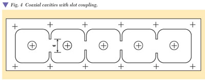
This structure yields a somewhat higher unloaded quality factor because more of the field is enclosed. The coupling between resonators is controlled via the width of the slot, w. The coupling coefficient between resonators may be determined by measurements of symmetrical-coupled resonators as a function of the slot width or via analysis of the self and mutual capacitance using an EM simulator. Both methods were employed and resulted in acceptable agreement, that is, less than 5 percent over the slot widths used in the filter, between the experimentally determined coefficients and the measured values as shown in Figure 5.

To illustrate the filter design procedure a PCS1900 transmit band filter (19301990 MHz) is required with minimum insertion loss (< 1.5 dB) and volume as the principal design specifications. A filter rejection of 60 dB, minimum, in the PCS1900 receive band (18501910 MHz) is also required.
From the earlier data, an eight-resonator filter is required to achieve the rejection requirements. This may be verified from direct calculation using
where
L(fa ) = the attenuation required at the specific rejection frequency fa
rdb = the in-band ripple factor
Δfn = the normalized bandwidth at the rejection frequency,
that is

Because the reject band is close to the passband, the passband was deliberately narrowed to 55 MHz so that coupling adjustment could be facilitated in order to increase the final filter bandwidth to 60 MHz. The filter parameters are
f0 = 1960 MHz
Δf = 55 MHz
n = 8
rdB = 0.05 dB

Qu = 2250

The LP prototype g-values are
g0 = 1.0000
g1 = 1.0437
g2 = 1.4514
g3 = 1.9899
g4 = 1.6502
g5 = 2.0457
g6 = 1.6053
g7 = 1.7992
g8 = 0.8419
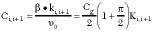
The coupling values are calculated using

The slot width may be determined from the measured coupling data of symmetrical coupled resonators or from an EM simulator that provides the capacitance matrix data for the particular structure. For this example, both techniques are utilized. First, the measured coupling data from a pair of symmetrical coupled resonators was subjected to polynomial regression of degree three. Next, the coefficients of the polynomial were used to generate an equation for the coupling coefficient as a function of the slot width. Finally, a plot of the coupling coefficient was used to determine the slot width for each coupled section.
The measured coupling data is displayed in Table 3 for three values of slot width for square cavities of 0.875 inches and center conductor diameters of 0.375 inches. These dimensions produce a resonator characteristic impedance of approximately 60 Ω.

Performing a polynomial regression produces an equation for the coupling coefficient Kc as a function of the slot width, w such that
Kc (w) = 0.02717 + 0.10865w 0.03150w2
The correlation coefficient R for the polynomial regression was 1.00.
Alternatively, an EM simulator may be utilized to determine the self-capacitance Cg and the mutual capacitance Cm for various slot widths. Subsequent data may also be subject to polynomial regression analysis to determine the correct slot width for each coupled resonator.
The susceptance slope parameter is calculated using
and the mutual coupling capacitors becomes
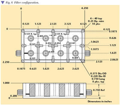
The filter configuration is shown in Figure 6. Note that all resonators are the same diameter and that coupling to the input and output is via direct "tap" or contact to the first and eighth resonator at a low impedance point on the resonators. Alternate coupling mechanisms are via capacitive probe at a high electric field point of the resonator or via transformer coupling. Generally, the tap is preferred because it eliminates the need for another machined part, provides a more compact filter, and makes the filter's input and output a direct short to ground at DC. The design data for the comb-line filter is listed in Table 4.

Filter Simulation
In order to conduct a simulation of the filter characteristics, an equivalent circuit is required. A suitable equivalent circuit may be constructed with the aid of the two-wire line equivalent of the coupled line shown in Figure 7.

If the coupled line equivalence is applied repeatedly, a complete filter equivalent circuit may be realized, as shown in Figure 8, where the tuning capacitance Ct , resonator quality factor Qu and external circuit coupling has been included. The complete filter was subjected to simulation and optimization using only the tuning capacitance and external coupling taps as the variable. The simulation results are shown in Figure 9.
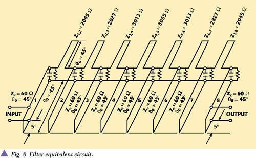

Note that the actual bandwidth is 52.8 MHz versus the design bandwidth of 55.0 MHz, and that the return loss is consistent with the 0.05 dB Chebishev response. The simulated midband insertion loss and group delay are 0.85 dB and 37.1 ns, respectively. The midband insertion loss and group delay estimates are
and
INTERDIGITAL BANDPASS FILTER ( /4-LINES)
The interdigital bandpass filter is another popular type of microwave filter implementation. They typically have lower loss than comb-line structures and are easier to tune. They require resonators that are fixed to ground at opposite sides of the supporting housing as shown in Figure 10. Therefore, the construction is not as suitable for manufacture as the comb-line filter.

In most cases, the resonator length is slightly shorter than /4 (typically, 0.9 /4), which allows the filter to be tuned to the center frequency with the tuning elements just breaking the cavity wall. This facilitates both ease of tuning and maximum unloaded quality factor Qu of each resonator. The coupling to the input and output is accomplished via contact at the low impedance point of the resonator.
The design procedure for interdigital bandpass filters is very similar to the comb-line filter design procedure. In this case, the example illustrates the design of a 500 MHz bandwidth filter centered at 10 GHz.
The filter parameters are
f0 = 10 GHz
Δf = 500 MHz
n = 5
rdB = 0.1 dB
 0 = π/4
Qu = 2500
Zc = 70 Ω
g0 = 1.0000
g1 = 1.1468
g2 = 1.3712
g3 = 1.9750
g4 = 1.3712
g5 = 1.1468
The coupling values are calculated using

the susceptance slope parameter becomes

and the mutual coupling capacitors are determined using

The calculation of the resonator coupling dimensions must be preceded by selection of the resonator ground plane spacing. In order to properly define a distributed resonator and reduce evanescent modes, certain geometric and aspect ratios must be maintained. It was found empirically that selection of ground plane spacing in accordance with

produced acceptable results.
The formula results from a resonator aspect ratio (ratio of length to diameter) of 2 x 1. The approximate ground plane spacing for a resonator characteristic impedance of 60 Ω is listed in Table 5.

For the present example, a ground plane spacing of 0.275" has been selected, which requires a resonator diameter of 0.128" to obtain a resonator characteristic of 60 Ω. This value is calculated from
Cristal2 has given the closed-form expressions for the even and odd mode capacitance per unit length for this line configuration, from which the self and mutual capacitance may be calculated (see Appendix A). The graph of the mutual capacitance versus resonator center-to-center spacing is shown in Figure 11.

The design data for the interdigital filter is listed in Table 6.

Filter Simulation
The equivalent circuit shown in Figure 12 is utilized to conduct a computer simulation. As in the case of the comb-line filter, a contact at the low impedance end of the resonator serves as the input and output coupling to the filter.
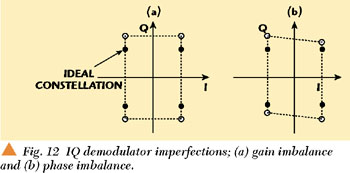
The results of the computer simulation using only the end capacitance and tap points as variables are shown in Figure 13. Note that the actual bandwidth is 467 MHz versus the design bandwidth of 500 MHz, and that the return loss is consistent with the 0.1 dB Chebishev response. The simulated midband insertion loss and group delay are 0.30 dB and 2.3 ns, respectively. The midband insertion loss and group delay estimates are

and
HALF WAVELENGTH VIA-HOLE COUPLED FILTER
This bandpass filter design example illustrates the utilization of series-type resonators coupled by impedance inverters. The general schematic of a bandpass filter, which employs series-type resonators coupled by impedance inverters, is shown in Figure 14.

The design procedure is similar to those previously explored. The filter parameters are
f0 = 10 GHz
Δf = 700 MHz
n = 5
rdB = 0.1 dB
g0 = g6 = 1.0000
g1 = 1.1468
g2 = 1.3712
g3 = 1.9750
g4 = 1.3712
g5 = 0.1468
The filter is constructed on 25 mil alumina (Al2 O3 ) substrate material (εr = 9.9). The available resonator quality factor for this type of filter is 750 if pure alumina with high quality metalization is employed. A schematic of the filter is shown in Figure 15.

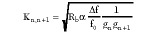
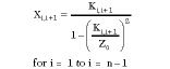
The resonator coupling values are calculated using
and the reactance slope parameter is

The impedance inverter values become
Ki,i+j = *ki,i+1 for i = 1 to i = n1
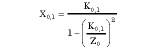
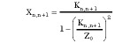
and the input and output inverter values are

and
The via-hole coupling reactance is calculated using
and
The coupling reactance is the result of the via-hole self-inductance, which is controlled by the via-hole diameter and/or number. The length of the resonators *n must be reduced by an amount commensurate with the magnitude of the coupling reactance using the equations
and

The actual via-hole diameter may be determined from the via-hole model within Series IV.™ This model was utilized to obtain data that was further refined using polynomial regression. The results are shown in Figure 16. The design procedure is very similar to the direct-coupled waveguide filter using inductive iris coupling found in Matthaei, Young and Jones.1

The filter data are listed in Table 7. The via-hole, half-wavelength, direct-coupled filter was simulated using the previously displayed equivalent circuit. The results are shown in Figure 17.


This via-hole, direct-coupled filter is particularly suited to wider bandwidth filters because the dimensions of the filter are more realizable than the side-coupled filters. There are also several implementations in addition to the microstrip medium, including stripline, finline, coplanar waveguide and slotline.
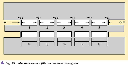
The implementation of the inductive reactance, direct-coupled filter in coplanar waveguide is shown in Figure 18. This implementation results in low insertion loss if an air-dielectric is utilized.
ACKNOWLEDGMENT
The principal reference for the content of this article is the work of Matthaei, Young and Jones.1 Many of the concepts within this reference have been investigated and interpreted in order to provide a greater intuitive understanding of the bandpass filter design process. This text is strongly recommended for those having little familiarity with this work. *
References
1. G.L. Matthaei, L. Young and E.M.T. Jones, Microwave Filters, Impedance-matching Networks and Coupling Structures, McGraw-Hill, New York, 1964.
2. E.G. Cristal, "Coupled Circular Cylindrical Rods Between Parallel Ground Planes," IEEE Transactions on Microwave Theory and Techniques, Vol. MTT-12, July 1964, pp. 428439.
3. W.J. Getsinger, "Coupled Rectangular Bars Between Parallel Plates," IRE Transactions on Microwave Theory and Techniques, Vol. MTT-10, January 1962, pp. 6572.
4. A.I. Zverev, Handbook of Filter Synthesis, John Wiley and Sons, New York, 1967.
5. G.L. Matthaei, "Interdigital Band Pass Filters," IEEE Transactions on Microwave Theory and Techniques, Vol. MTT-10, No. 6, November 1962.
6. G.L. Matthaei, "Comb-line Band Pass Filters of Narrow or Moderate Bandwidth," Microwave Journal, August 1963.
7. S.B. Cohn, "Parallel-coupled Transmission-line-Resonator Filters," IEEE Transactions on Microwave Theory and Techniques, Volume MTT-6, No. 2, April 1958.
8. R.M. Kurzrok, "Design of Comb-line Band Pass Filters," IEEE Transactions on Microwave Theory and Techniques, Vol. MTT-14, July 1966, pp. 351353.
9. M. Dishal, "A Simple Design Procedure for Small Percentage Round Rod Interdigital Filters," IEEE Transactions on Microwave Theory and Techniques, Vol. MTT-13, September 1965, pp. 696698.
10. S.B. Cohn, "Dissipation Loss in Multiple-coupled-resonator Filters," Proceedings of the IRE, Vol. 47, August 1959, pp. 13421348.
 Kenneth V. Puglia holds the title of Distinguished Fellow of Technology at the M/A-COM division of Tyco Electronics. He received the degrees of BSEE (1965) and MSEE (1971) from the University of Massachusetts and Northeastern University, respectively. He has worked in the field of microwave and millimeter-wave technology for 35 years, and has authored or co-authored over 30 technical papers in the field of microwave and millimeter-wave subsystems. Since joining M/A-COM in 1971, he has designed several microwave components and subsystems for a variety of signal generation and processing applications in the field of radar and communications systems. As part of a European assignment, he developed a high resolution radar sensor for a number of industrial and commercial applications. This sensor features the ability to determine object range, bearing and normal velocity in a
multi-object, multi-sensor environment using very low transmit power. Puglia has been a member of the IEEE, Professional Group on Microwave Theory and Techniques since 1965.
APPENDIX A
NORMALIZED SELF AND MUTUAL CAPACITANCE OF ROUND RODS BETWEEN PARALLEL GROUND PLANES
Upon completion of specific elements of the design procedure and the calculation of the normalized self and mutual capacitance per unit length, rod diameter and center-to-center spacing may be calculated. First, the filter ground plane spacing h must be selected. The selection of a suitable ground plane spacing is bounded by the out-of-band spurious response, passband frequency and insertion loss. Certainly, the ground plane dimension should be less than one quarter wavelength and no smaller than that required to achieve an unloaded Qu consistent with the insertion loss requirements. The maximum ground plane spacing may be estimated in accordance with

This formula provides the approximate values for ground plane spacing listed in Table A1:

Cristal2 has given the closed-form expressions for the even and odd mode capacitance per unit length from which the self and mutual capacitance may be calculated from
and
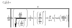
For reasonable accuracy, the parameter m may be limited to 100. The self and mutual capacitance is calculated using1
Cg (c) = Ce (c)
and
Cm (c) = 0.25[C0 (c)Ce (c)]
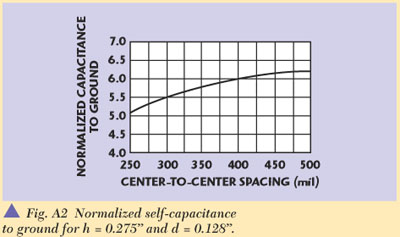
The equations have been programmed using Mathcad for a ground plane spacing of 0.275 inches and a rod diameter of 0.128 inches, that is, Zo = 60 Ω. The data are shown in Figures A1 and A2.

APPENDIX B
ALTERNATE FILTER IMPLEMENTATIONS
In addition to the examples within Part II of this tutorial, there are several alternative filter implementations that lend themselves to the general design procedure and should be cited. These alternative filter implementations utilize resonators not fully exploited in recent literature and for which recent CAD tools have permitted extensive analysis and understanding. Two specific types of resonators are suggested for special applications: cylindrical dielectric resonators and helical resonators.
DIELECTRIC RESONATOR FILTER
Figure B1 shows the electrical and mechanical schematic of a three-section bandpass filter using cylindrical dielectric resonators. Resonators of this type are not typical of conventional lumped or distributed element structures due to the existence of multiple resonant frequencies or modes. This resonator type permits the design of narrowband, low loss filters due to the high unloaded quality factor (Qu > 10,000) in the principal or dominant resonant mode.

A note of caution is in order with respect to the multiple resonator modes and the environment necessary to suppress excitation of these modes and thereby eliminate loss spikes and spurious responses in the filter transfer function. There are two techniques suitable for such a determination. The first technique requires experimental characterization of the resonator modes and mode coupling via the methods described in Part I. The second, and until recently more difficult analysis, involves analytical determination of the modes and mode coupling through the utilization of a three-dimensional electromagnetic simulation tool. Some sophisticated filter designers have made use of auxiliary modes to design so-called dual-mode or multi-mode filters that utilize two or more of the resonant modes to obtain very compact, low loss filters with excellent rejection band characteristics. The general design procedure is not suitable for this task.
The input, output and inter-resonator coupling is accomplished via the magnetic field which is orthogonal to the circular plane of the cylindrical resonator for the dominant TE01* mode. The equivalent circuit of the dielectric resonator filter represents the electrical behavior in the principal mode only. It has acceptable accuracy if the resonator environment and mounting arrangement has demonstrated elimination of the auxiliary modes.
To obtain the highest unloaded quality factor available from the cylindrical dielectric resonator, a low loss dielectric support structure is required to separate the resonator from the electrical ground boundary.
HELICAL RESONATOR FILTER
The helical resonator filter is another filter type for which the general design procedure is applicable. Helical resonator filters are particularly useful within the VHF and UHF bands for low loss, narrowband applications, and where the greater volume of a distributed resonator filter is prohibitive. The helical resonator is at least partially distributed due to the combination of self-inductance and the electrical length of the coil structure. The helical resonator is tuned via the distributed capacitance of the tuning screw at the high electric field point of the resonator. A direct tap at the low electric field point of the resonator accomplishes input and output coupling. The resonator spacing and coupling slot at the high magnetic field point of the helical structure facilitates inter-resonator coupling.
Figure B2 shows the mechanical and electrical schematic of a typical five-section helical resonator filter. Once again, resonator parameters and coupling coefficients may be determined experimentally or analytically by the use of EM simulation tools. Usually, a low loss dielectric form that facilitates uniformity, placement and structure supports the helical resonator.
