
A DC to Ka-band Low Cost Surface Mountable RF-VIA™ Package
Kyocera America Inc.
San Diego, CA
 The wireless market, including cellular phones, local multipoint distribution systems, point-to-point radio programs, broadcasting systems and data exchange systems (such as Bluetooth), is experiencing explosive growth. As the number of subscribers grow, the demand for high speed transmission capacity continues to increase.
The frequencies used for local multipoint distribution system (LMDS), point-to-multipoint, point-to-point radio and satellite communications fall into the 22 to 42 GHz range. This demands a high performance package, which is also low cost and suitable for assembly in high volume. Among conventional millimeter-wave packages, the metal wall package provides excellent electrical performance, such as 1 dB (S21 ) for 90 to 100 GHz.1,2 This performance has been achieved by using material properties of ceramics in combination with package design optimization. Using this expertise, the RF-VIA™ low cost, miniature, lightweight, surface mountable package has been developed with excellent RF characteristics.
THE PACKAGE STRUCTURE
To fulfill the market requirements three objectives were followed: the package had to be a low cost solution, with easy board level mounting and high reliability (package level and board level). Figure 1 shows the structure of RF-VIA package in a lead frame. The package features surface mounting, metal die attach pad (with an optional ceramic die attach pad), hermeticity and low cost, and is supplied in the form of a leadframe strip.

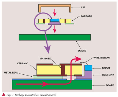
To reduce the package cost, the package structure has been simplified and the package size reduced. The RF-VIA package consists of a single layer of ceramic (alumina) and metal leadframe. For devices requiring significant heat dissipation the package is offered with a metal die attach pad, such as Cu, CuW and CuMo, as shown in Figure 2. Hermeticity is achieved by using a metal lid with a AuSn solder preform. An epoxy sealed ceramic lid is available where hermeticity is not required. This package can be board-mounted just as any other surface-mount technology (SMT) components (such as capacitors, resistors and inductors), as shown in Figure 3. Table 1 lists the metal options available and their properties.


The package leadframe serves an important function in obtaining the required RF performance. A ball grid array (BGA)-type package exhibits significant performance variability at high frequencies due to the variation in ball height. In contrast, a leadframe-type package has a stable height due to the fixed leadframe thickness. Electrically, the leadframe does not add inductance in the signal path if the lead is cut close to the edge of the package body. The leadframe-type package can be effectively used in volume manufacturing because the package is supplied in strip format. This configuration allows a high degree of assembly automation.
THE PACKAGE DESIGN
In conventional surface-mount packages, a device is mounted on the die attach area of the package and wire-, ribbon- or flip chip-bonded for electrical connection. The electrical signal goes through the via holes to the backside of the package for board-mounting. Measurements on this type of package show that such a package has greater than 1 dB insertion loss per port above 10 GHz due to impedance mismatch, as shown in Figure 4.

The superior performance of the RF-VIA package is due to the optimized number and locations of ground via holes around the signal trace/via hole. In addition to the impedance matching, the inductance values of the via hole and top and bottom ground layers must be optimized. This was accomplished by using the equivalent circuit shown in Figure 5.

In performing package design optimization, the following items, as shown in Figure 6, need to be considered for improvement: the gap between signal line and ground pattern (capacitance), the number of ground via holes (inductance), and the location of the signal via hole with respect to the ground via holes (impedance matching). To verify the package performance, the characteristics of two samples were measured. One of the samples has been built as a standard RF-VIA package with a through-line insert (built as a 50 Ω coplanar structure), while the other sample has been built as a test substrate (instead of a die cavity it has a 50 Ω line printed on the top layer). Figure 7 shows the design of test package and test substrate.


For measurements, a ground-signal-ground (GSG) probe was directly attached to lead pads on the bottom side. Figure 8 shows the measurement results of the test package and test insert. At frequencies over 35 GHz the insertion loss characteristics for the test package and test substrate are very close. Figure 9 shows the results of a simulation for an optimized design superimposed on the measurement results. According to simulation results, the resonant frequency at 27 GHz is decreased, and insertion loss at 38 GHz is approximately 1 dB.3


A second set of test units were manufactured per the optimized package design, and the measurements for these parts are shown in Figure 10. At 33GHz, an insertion loss of approximately 1 dB is achieved (including the through-line, one gold ribbon bond, package and test board).

RELIABILITY
Reliability of the RF-VIA package has been assessed at both the board and package level. The package level reliability has been assessed by performing tests per EIAJ, while at the board level the package has been tested per MIL-STD-883D. Test results are listed in Tables 2 and 3.


FURTHER IMPROVEMENTS
Measurements on test packages show an insertion loss of 1.4 dB at 40 GHz. The measurement includes two signal vias and a through line. Therefore, insertion losses of less than 1 dB per port have been achieved (including the board). Further design optimization will be performed to reduce the capacitance at the lead attachment pads by layer structure modification and for via hole location optimization considering the board design. In addition, continuous improvements in the properties of ceramic or metallization materials are expected to contribute to the package performance improvements.
CONCLUSION
A low cost RF-VIA package has been developed that exhibits lower than 1 dB insertion loss up to 33 GHz. Further work is being conducted to extend this performance to the 40 GHz frequency range. Excellent board and package level reliability have been demonstrated.
References
1. S. Tomie, S. Morioka, Y. Sawa and T. Okumichi, "Development of Millimeter-wave Package at 94 GHz," APMC'98 Proceedings, December 1998, pp. 289293.
2. T. Okumichi, S. Tomie and M. Fujii, "Development of Millimeter-wave Package for W-band," European Microwave Conference '98, October 1998.
3. S. Morioka and Y. Sawa, "Surface Mount Package for High Frequency Band," APMC '99 Proceedings, December 1999, pp. 958961.
Kyocera America Inc.
San Diego, CA
Circle No. 302