
Two push-push MMIC fixed frequency oscillators operating at G-Band are fabricated using 0.8 μm InP double heterojunction bipolar transistor (DHBT) technology with peak ft and fmax of 150 and 230 GHz, respectively. The push-push architecture of each oscillator consists of two sub-oscillators based on a modified Colpitts configuration. Even-mode oscillation is inhibited, and the second harmonic is extracted at the collector node. The first oscillator delivers an output power of −6 dBm at 161.6 GHz, and the second delivers an output power of −25 dBm at 204.8 GHz.
mmWave and sub-mmWave MMIC frequency sources above 100 GHz are essential building blocks for communication, radar, medical and automotive imaging systems due to the short wavelengths at these frequencies and, consequently, the wide bandwidths that can be achieved.1-2 Several designs have been published, which include a fundamental mode oscillator,3 an oscillator-doubler hybrid architecture4 and a push-push oscillator.5 Of these approaches, the push-push approach is more attractive for high frequency VCO design.6 InP DHBT device technology offers a high breakdown voltage and high power capabilities, as well as outstanding high frequency properties,7 making it a good candidate for frequency sources in this frequency range, as has been well demonstrated.4
The primary requirement for high frequency signal sources is high output power, which is desired in many applications such as automotive radar.8max of the transistor, transistor gain is very low, which makes it difficult to achieve oscillation. The goal is to reach a high oscillation frequency with sufficient output power. To enable oscillator operation near its limit, in terms of frequency (ft and fmax ), a push-push topology is often used with two common-base sub-oscillators operating at half frequency.
This article describes the design of two push-push G-Band oscillators using 0.8 μm InP DHBT technology with peak ft and fmax of 150 and 230 GHz, respectively. The first oscillator (OSC I) delivers ‐ 6 dBm output power at 161.6 GHz, while the second (OSC II) delivers −25 dBm output power at 204.8 GHz.
InP DHBT TECHNOLOGY
InP DHBT technology with an emitter width of 0.8 μm is used in the fabrication of the oscillators. The transistors are grown on a 3-inch InP wafer with an epitaxial profile designed for high frequency. The epitaxial layers consist of a 40 nm carbon-doped base layer and a composite collector.9 Measured S-parameters of the 0.8 × 10 μm2 DHBT demonstrate ft and fmax of 150 and 230 GHz, respectively, at a bias of IC = 14 mA and VCE = 1.5 V. The device breakdown voltage BVceo is greater than 5 V.
The InP DHBT MMIC process includes MIM capacitors, thin film resistors (50 Ω/square), three levels of metal (M1, M2, M3), benzocyclobutene (BCB) passivation and wafer planarization after device formation. Microstrip is employed for low loss. A micro- photograph of the MMIC is shown in Figure 1. The layout is symmetric, with a total chip size of only 560 × 450 μm2, including the DC and RF probe pads.
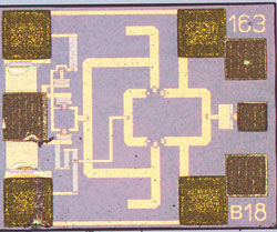
Figure 1 Oscillator IC.
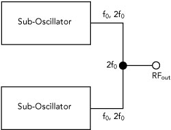
Figure 2 Principle of a push-push oscillator.
CIRCUIT DESIGN
The push-push approach em- ploys a symmetric topology operating differentially at the fundamental mode, as shown in Figure 2. Virtual grounds are created for the fundamental signal and all odd harmonics at the symmetry plane, while the even harmonics add in phase. Both of the two G-Band push-push oscillators are based on the schematic circuit diagram shown in Figure 3. It consists of two identical Colpitts sub-oscillators operating at half the desired frequency. In one of the sub-oscillators, an inductive transmission line (Lb) below a quarter wavelength provides series positive feedback, which helps produce a negative impedance when looking into the transistor emitter and collector.10 The open stub, Lo, acts like a capacitance, which also serves as a destabilizing element. Compared with the commonly used Colpitts designed for low frequency operation, a modified version with an added inductive transmission line (Le) employed to improve high frequency performance.
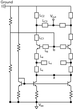
Figure 3 Push-push oscillator schematic.
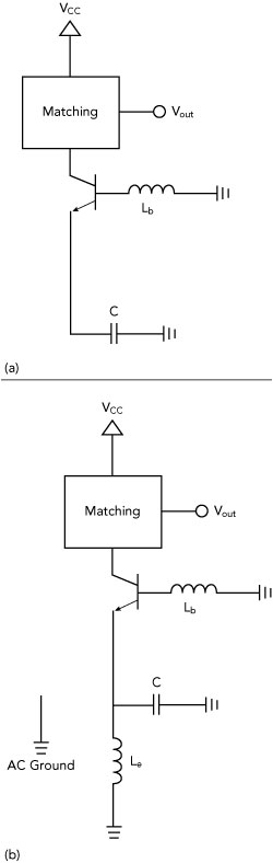
Figure 4 Simplified Colpitts oscillator (a), modified for high frequency operation (b).
Figure 4a is a simplified diagram of a Colpitts oscillator, and Figure 4b shows the modified version, with Le for high frequency operation. In simulation, the additional inductive element boosts negative resistance at higher frequencies. The effect of Le on the real part of the impedance looking into the DHBT collector is shown in Figure 5. Consequently, the oscillation frequency is shifted higher.
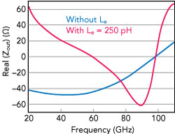
Figure 5 Simulated real part of the impedance looking into the DHBT collector.
The fundamental frequency of the push-push oscillator is set mainly by the resonators consisting of Lb, Le and Lo. In this work, the two oscillators are fabricated with different resonator lengths Lb, Le and Lo, for different oscillation frequencies. To ensure proper push-push operation, each sub-oscillator must oscillate in the odd mode and inhibit even-mode oscillation. In Figure 3, the fundamental signals of the two sub-oscillators at points a and b are out of phase, while the second harmonics add in phase; i.e., the fundamental signal is suppressed, and the second harmonic is easily extracted.
The second harmonic signal can be extracted from the base, emitter or collector; however, higher output power is obtained at the collector, since the signal swing is larger. The breakdown voltage of the DHBT is larger than 5 V, which provides good potential for higher output power. The largest signal swing and highest output power are obtained by directly shorting the differential output.10 In this paper, a harmonic matching technique is employed to enhance output power. A T-shaped, second harmonic impedance matching network is attached to the collector for each sub-oscillator. According to simulation, the output matching network—especially the shorted stub Lc2—affects output power significantly. With optimization of the matching network, output power at the second harmonic is increased by 5 dB.
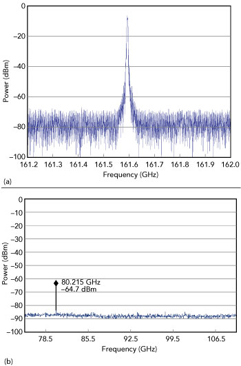
Figure 6 Measured second harmonic (a) and fundamental frequency (b) of OSC I. The measurement of the fundamental includes 37 dB loss from the W-Band harmonic mixer used for on-wafer test.
The push-push oscillator MMIC topology enables a compact chip size that is much smaller than an oscillator-multiplier hybrid architecture. All DHBTs have 0.8 × 10 μm2 emitters. Circuit simulation is performed using Keysight’s Advanced Design System (ADS). Small-signal S-parameter analysis is used to determine the oscillation frequency; harmonic balance and transient analyses are performed to ensure oscillator functionality, and post layout simulation is performed with the Momentum 2.5D planar EM simulator.
MEASURED RESULTS AND DISCUSSION
The oscillators are characterized in two steps at room temperature. The fundamental signal measurement is done on-wafer. Spectral measurements are performed using a Keysight N9030A PXA signal analyzer extended in frequency with a W-Band harmonic mixer. The second harmonic measurement is done with the oscillator chips installed in modules. A G-Band harmonic mixer is used to extend the signal analyzer frequency range.
Figure 6 shows the measured spectrum of OSC I at the second harmonic and fundamental. OSC I delivers an output power of −6 dBm to a 50 Ω load at 161.6 GHz, while the fundamental signal output power is only ‐ 27 dBm (i.e., 21 dBc fundamental suppression). The circuit employs a single supply voltage Vee = ‐ 3 V with a total current drain of approximately 40 mA; the bias current mirrors consume more than half the DC power. The oscillator core consumes about 45 mW, corresponding to a DC-to-RF efficiency of 0.56 percent. OSC II delivers an output power of −25 dBm at 204.8 GHz. The output power is low because the oscillation frequency is very close to the transistor ’s fmax
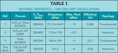
Table 1 lists several reported HBT-based oscillators operating above 100 GHz. This design at 161.6 GHz achieves higher output power than the others, at close to fmax. This is attributed to the modified Colpitts topology and the harmonic matching technique.
CONCLUSION
Two monolithically integrated harmonic oscillators operating at G- Band use a push-push Colpitts topology and harmonic matching to operate at frequencies close to the transistor fmax. The output power of the two oscillators is −6 dBm at 161.6 GHz and −25 dBm at 204.8 GHz. DC-to-RF efficiency of OSC I at 161.6 GHz is 0.56 percent after subtracting the DC power consumption of the bias current mirrors.
ACKNOWLEDGMENTS
This project was supported by the Chinese Academy of Sciences The World Academy of Sciences (CAS-TWAS) president fellowship program, a program of the National Natural Science Foundation of China (Grant No. 61434006) and the National Natural Science Foundation of China (Grant No. 61401457).
References
- A. Arbabian, S. Callender, S. Kang, M. Rangwala and A. M. Niknejad, “A 94 GHz mmWave-to-Baseband Pulsed-Radar Transceiver with Applications in Imaging and Gesture Recognition,” IEEE Journal of Solid-State Circuits], Vol. 48, No. 4, April 2013, pp. 1055–1071.
- M. Urteaga, A. Carter, Z. Griffith, R. Pier- son, J. Bergman, A. Arias, P. Rowell, J. Hacker, B. Brar and M. J. W. Rodwell, “THz Bandwidth InP HBT Technologies and Heterogeneous Integration with Si CMOS,” IEEE Bipolar/BiCMOS Circuits and Technology Meeting, September 2016, pp. 35–41.
- Y. Zhao, B. Heinemann and U. R. Pfeiffer, “Fundamental Mode Colpitts VCOs at 115 and 165 GHz,” IEEE Bipolar/BiCMOS Circuits and Technology Meeting, October 2011, pp. 33–36.
- R. Kozhuharov, M. Bao, M. Gavell and H. Zirath, “A W- and G-Band MMIC Source Using InP HBT Technology,” IEEE MTT-S International Microwave Symposium Digest, June 2012, pp. 1–3.
- P. Y. Chiang, O. Momeni and P. Heydari, “ A 200 GHz Inductively Tuned VCO with 7 dBm Output Power in 130 nm SiGe BiCMOS,” IEEE Transactions on Microwave Theory and Techniques, Vol. 61, No. 10, October 2013, pp. 3666–3673.
- C. H. Jeong, C. Kwon, S. C. Park and S. W. Kim, “ Design of Push-Push Voltage-Controlled Oscillator for D-Band Applications,” 2014 IEEE International Conference on Ultra-WideBand, September 2014, pp. 327–330.
- J. Ge, Y. Cao, D. Wu, Y. B. Su, Z. Jin and X. Liu, “A Combined Model with Electrothermal Coupling and Electromagnetic Simulation for Microwave Multifinger InP-Based DHBTs,” IEEE Transactions on Electron Devices, Vol. 59, No. 3, March 2012, pp. 673–679.
- J. Yun, N. Kim, D. Yoon, H. Kim, S. Jeon and J. S. Rieh, “A 248–262 GHz InP HBT VCO with Interesting Tuning Behavior,” IEEE Microwave and Wireless Components Letters, Vol. 24, No. 8, August 2014, pp. 560–562.
- Y. H. Zong, Y. B. Su, Z. Jin, X. T. Wang, Y. X. Cao, H. F. Yao, X. X. Ning, Y. M. Zang and X. Y. Liu, “An InGaAs /InP W-Band Dynamic Frequency Divider,”Journal of Infrared and Millimeter Waves, Vol. 31, No. 5, October 2012, pp. 393–398.
- M. Hossain, N. Weimann, V. Krozer and W. Heinrich, “A 315 GHz Reflection-Type Push-Push Oscillator in InP-DHBT Technology,” 46th European Microwave Conference, October 2016, pp. 485–488.
- M. Jahn, K. Aufinger, T. F. Meister and A. Stelzer, “125 to 181 GHz Fundamental Wave VCO Chips in SiGe Technology,” IEEE Radio Frequency Integrated Circuits Symposium, June 2012, pp. 87–90.