
MCHEM Hardware
Ettus X310 + 2x UBX 160 Daughter Cards
- Wide frequency range: 10 MHz to 6 GHz
- Wide bandwidth: up to 160 MHz
- USRP compatibility: X Series
- RF shielding
- Full duplex operation with independent Tx and Rx frequencies
- Synthesizer synchronization for applications requiring coherent or phase-aligned operation
- Dual 10 GbE interfaces
- Large customizable Xilinx Kintex-7 FPGA for high performance DSP (XC7K410T) ATCA-3671
- 4 Virtex-7 690T FPGAs with a combined 14,400 DSP slices
- 64 GB onboard DDR3 DRAM
- 4 ATCA IO (AIO) module slots with both analog and high speed serial I/O options
- Up to 1.5 Tbps external connectivity available through PCI Express, SFP+ and QSFP
- Programmable with the LabVIEW FPGA Module or BEEcube Platform Studio software
MAPPING THE MCHEM ONTO HARDWARE
Using the parameters from the previous section, Colosseum’s MCHEM is mapped onto hardware (see Figure 1). From the image, we note the need for 256 RF inputs and outputs. MCHEM achieves this by using 128 USRP X310 radios populated with UBX RF daughterboards (see sidebar), each with two transmit and two receive channels, thus creating 256 in total. These radios are responsible for digitizing the RF and passing it on to the channel emulating backbone, which does FIR filter-based computation. The channel emulation’s heavy lifting is handled by 16 ATCA-3671 accelerator blades (see sidebar). Each ATCA-3671 has four Virtex-7 FPGAs, 64 FPGAs in total, to meet the requirements.
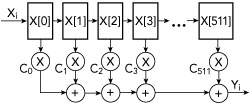
Figure 4 Dense 511-tap FIR filter, requiring 511 complex-value multiplies, 510 complex-value adds, storage and routing for all the coefficients.
The system is organized into four groups, or quadrants, of 64 inputs and outputs powered by four accelerator blades (16 FPGAs). Each quadrant has a powerful ×86 Dell server that handles command-and- control and loading of the channel coefficients into the emulator. The radios and accelerators in each quadrant connect to the server via 10 Gigabit Ethernet distributed through a layer-2 Dell Ethernet switch.
The biggest challenges to digitally emulating the interactions of the physical world lie in the computational burden. The chosen MCHEM hardware has 64 total FPGAs available to bear the weight of this burden. At first blush, this may seem like overkill, but in fact this is not actually sufficient for a naïve implementation of channel emulation. Without some key observations about the structure of the math behind the underlying model, resulting optimizations in data movement, computation and key architectural and implementation choices, this problem could not be solved with the chosen hardware.
FIR filters, like those at the core of our design, normally operate at the system sample rate, which in our case is 100 MSPS. Figure 4 shows a “dense” 511-tap FIR filter with delay elements of 10 ns, which is the delay between consecutive samples. The resources required to build such a large filter are substantial and would quickly exhaust those in our 64 FPGAs. The solution is to use a sparse FIR filter, as shown in Figure 5. Here the resources are dramatically reduced because most of the multipliers and adders present in a fully populated FIR filter are not used.
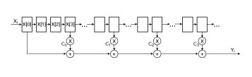
Figure 5 Sparse FIR filter design with 511 delay elements and four sparse taps, requiring four complex-value multiplies, three complex-value adds, storage and routing for the four coefficients.
The key FIR filter computation is a series of complex-valued multiply accumulates (CMAC). This maps well to the DSP slices in our core FPGAs. A CMAC can be implemented using three real multiply ac- cumulates (MAC). Each 4-tap FIR filter thus needs to perform 12 MACs. Using the sparse FIR filter as the core DSP component, the overarching design can now be viewed as a large array of tiled sparse FIR filters and adders, as shown in Figure 6. In total, 65,536 filters are needed for the 256 inputs and outputs. This equates to 786,432 MACs per sample, 78.6432 TMAC/s or 157 TOps. Each ATCA accelerator blade consists of four Virtex-7 FPGAs with a total of 14,400 DSP blocks.
Assuming that the DSP blocks are running at the system sample rate (100 MHz), then we would re- quire over 50 accelerator blades (200 FPGAs) to do the computation in real-time! However, by over-clocking the FGPA by a factor of four (i.e., running it at 400 MHz) it is possible to get the computation to fit into our 64 FPGAs. The lingering question, however, is how to get the data where and when it is needed to effectively use all 64 FPGAs.
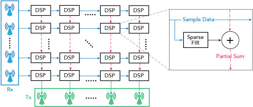
Figure 6 MCHEM’s core digital signal processing as an array of tiled sparse FIR filters and adders.
DATA MOVEMENT TOPOLOGY
Now that we know the cadre of 64 FPGAs is capable of handling the computational needs of our wireless channel model, we must address the challenge of moving all this digital data between the 64 FPGAs. Using the most straightforward approach to compute one transmitter’s contribution to each of the 256 receivers, we need to co-locate (i.e., copy) the data from all the channels before even attempting to process it. That means getting 102.4 GB/s of time- aligned sample data in one place for processing, just for one channel out of 256 (or a total data band- width of 26.2 TB/s)! To effectively partition the computation among the 64 FPGAs, we must divide-and- conquer to reduce the required I/O bandwidth to a tenable level.
To address the challenge of data movement we have to understand the physical connectivity between the 64 FPGAs. From Figure 7, we see that each Virtex-7 FPGA in one of the accelerators connects to two radios, where each radio has two channels. Thus, each FPGA is responsible for four inputs and four outputs. Each accelerator blade has four FPGAs that are connected in a 2 × 2 mesh con- figuration using printed circuit board traces. The four FPGA accelerators within a single quadrant are connect- ed in the same 2 × 2 mesh topology using QSFP+ cables (see Figure 8).
Figure 7 FPGA connectivity to the radio interface (USRP X310).
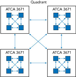
Figure 8 FPGA accelerator (ATCA 3671) connectivity within one quadrant.
To reign in the data movement requirements, consider the data needs of a single FPGA. We will enumerate the FPGAs as FQAN, where Q is the quadrant where the FPGA resides, A is the accelerator blade where the FPGA resides and N is the FPGA number. A depiction of all 64 FPGAs are shown and labeled in Figure 9.
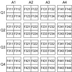
Figure 9 MCHEM’s 64 FPGAs enumerated by quadrant, accelerator blade and FPGA number.
Recall that the FPGA receives four input channels but needs the data from all 256 channels before computing its four outputs. From FPGA F111’s perspective, for example, to acquire all necessary data, we must follow a series of data movement steps:
Step 1—Acquire RF data from the four radios directly connected to us.
Step 2—Share the four channels of data with FPGAs in other accelerator blades in our quadrant (F121, F131 and F141). We have just shared data along the X dimension in our three dimensional topology, and we are now in possession of 16 channels of data.
Step 3—Share our 16 channels of data with FPGAs in the same ac- celerator (F112, F113, F114), which transfers data along the Y dimension. All FPGAs in quadrant 1 are now in possession of 64 channels of data.
At this point in the process, due to bandwidth restrictions, we can- not continue this same process to acquire the remaining 192 channels. However, we can take advantage of the structure of the channel-model- ing problem to reduce the data we need to transmit. Consider the fol- lowing: if we sent all 64 channels of data to quadrant 2’s FPGA (F211), after applying the appropriate FIR filters, F211 would simply sum all the outputs of the filters. So rather than send all 64 channels of data, we can apply the same FIR filters to the 64 channels we currently have, sum the result and send only the sum, reducing the data transmission by 64x. Doing this allows us to move onto the next step.
Step 4—Apply the appropriate FIR filters to channels 1 to 64, summing the result to produce a 64 channel partial sum. Also, compute the 64 chan- nel partial sums for F211, F311 and F411.
Step 5—Share the partial sum with F211, F311 and F411 and receive the respective sums from them. We have now shared across the Z dimension and we are in possession of 256 channels worth of partial sums.
Step 6—Add up all the partial sums computed locally and received from other FPGAs. We are now in possession of the final data streams for the four directly connected radio channels.
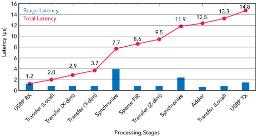
Figure 10 Simulated network latency, showing the delay for each hop as data moves through MCHEM.
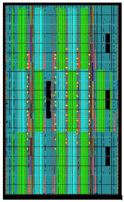
Figure 11 MCHEM FPGA “floor plan.”
Step 7—Transfer the data to the appropriate radios and transmit out the RF ports.
Of course, there is no free lunch. As shown in Figure 10, all of these data movement steps cost time and incur a latency of approximately 15 μs.
IMPLEMENTING THE FIRMWARE DESIGN
Now that we can get all the data where it needs to be, we still need to synthesize an FPGA image that fits the requisite number of FIR filters in each FPGA. We divide the 65,536 sparse FIR filters across the 64 FPGAs for a total of 1,024 filters per FPGA, resulting in almost 90 percent of the DSP resources and about 80 percent of RAM resources being used in each FPGA. Anyone
familiar with FPGA design will realize that a design with such high re- source utilization and a high clock rate (400 MHz) is extremely difficult to implement in a repeatable way while still satisfying all functionality, timing and power constraints. For that reason, the FIR filter block had to be hand crafted and the filter array, which is just a collection of filter blocks, had to be hand placed on the chip. The equivalent challenge in a strictly software paradigm would be creating a very tight assembly code routine to achieve the highest possible performance.
Figure 11 shows the completed FPGA design. The filter blocks are highlighted in green and cyan. The final per FPGA utilization numbers are shown in Figure 12. As a consequence of how the design was decmposed and given the symmetry of data movement throughout the system, each of the 64 FPGAs in the system runs with the exact same FPGA image. This greatly reduces overall design complexity.
LIFE AFTER SC2
It should be evident that Colosseum is likely to remain one of the largest and most powerful channel emulators on the planet for some time. After DARPA’s SC2 has completed, Colosseum will hopefully enter service as a testbed for the research community, enabling researchers across the U.S. to continue to pose and address challenging problems that cannot be effectively answered using limited, small-scale experimentation.
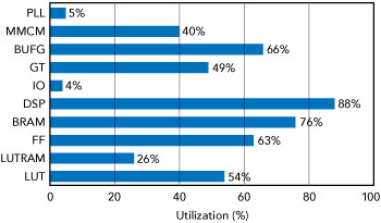
Figure 12 FPGA utilization.
In this article, we have introduced the need for, and shown the achievability of large-scale, controlled experimentation and testing of burgeoning wireless communication concepts. We hope continued avail- ability of this testbed and perhaps future testbeds like it will engender renewed and expanded research in spectrum autonomy and other new challenging wireless endeavors.
Reference
- “Cisco Visual Networking Index: Global Mobile Data Traffic Forecast Update, 2016–2021 White Paper,” Cisco, March 2017, www.cisco.com/c/en/us/solutions/ collateral/service-provider/visual-net- working-index-vni/mobile-white-paper- c11-520862.html.