
A monolithic U-Band, stacked InP heterojunction bipolar transistor (HBT) power amplifier (PA) demonstrates a saturated output power of 26 dBm, a compact chip size of 0.88 mm × 0.67 mm and a maximum power-added efficiency (PAE) of 28.7 percent at 52 GHz. Its output power density of 670.1 mW/mm2 is higher than other reported U-Band HBT PAs. An active biasing topology is used to enhance PAE and linearity.
PAs play an important role in wireless systems, not only because they are principal drivers of system performance, they also consume large amounts of prime power while generating heat and producing noise and interference.1-3 High efficiency PAs are especially vital for portable devices because of limited battery capacity.
The solid state III-V compound semiconductor HBT leverages material properties for high efficiency PA applications; however, its low collector-emitter breakdown voltage (BVCEO) is a major drawback. Methods proposed to overcome this include:
- A stacked topology: high speed device for a common emitter (CE) and a high breakdown device for a common base (CB) to generated high gain and high output power.4
- A CB topology5-6 to increase the voltage swing to obtain high output power, because the collector-base breakdown voltage is higher than the collector-emitter breakdown voltage.
- Passive network compensation7 to increase the effective collector-emitter breakdown voltage.
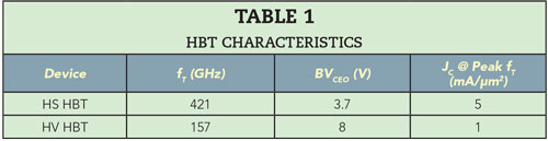
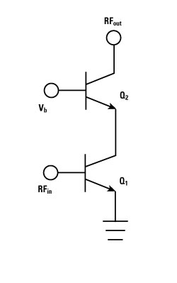
Figure 1 Stacked HBT PA with two transistors.
In this article, we describe a fully matched, stacked PA MMIC with an active bias circuit using only high speed HBTs. It is small in size, exhibiting a 670.1 mW/mm2 output power density and 28.7 percent PAE. To our knowledge, this is the highest output power density demonstrated by an InP HBT PA.
InP HBT STACKED CONFIGURATION
The stacked structure, comprised of a CE with high speed HBTs and a CB with high breakdown voltage HBTs, is generally used because the collector-base breakdown voltage is higher than the collector-emitter breakdown voltage. Generally, the peak current density for the high speed HBT is 2 to 10× greater than that of the high voltage devices. Because the collector current of both HBTs should be the same, the emitter area of the high voltage HBTs is several times larger than that of the high speed HBTs.
Table 1 shows high speed and high voltage HBT characteristics for the 0.5 μm InP HBT process. The 8 V BVCEO of the high voltage HBT is helpful for high output power, but the peak current density is 5× smaller than that of a high speed HBT, requiring a 5× larger emitter area. So the output power, PAE and output power density of the high speed HBT are higher than those of the high voltage HBT with the same emitter area. In this work, we use only high speed HBTs for the cascode configuration, to reduce MMIC size and simultaneously maximize PAE and output power.
The U-Band stacked PA is designed using a commercial 0.5 μm InP HBT process. The schematic of the two-stacked PA is shown in Figure 1.
Figure 2 shows the small-signal equivalent circuit of transistors Q1 and Q2 in the stacked configuration of Figure 1. The output resistance looking into the collector of Q1 is given by
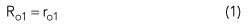
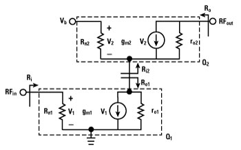
Figure 2 Small-signal equivalent circuit for transistors Q1 and Q2 in the stacked configuration.
and the input resistance looking into the emitter of Q2 is
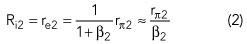
The voltage gain for the first stage is given as
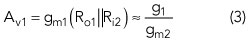
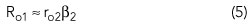
The total output resistance of the cascode structure is given as
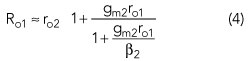
Since gm2ro1 >> β2 and β2 >> 1, Equation 4 can be simplified to
The total transconductance of the stacked structure is given b
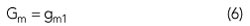
From Equations 5 and 6, the total voltage gain Av for the cascode structure can be expressed as
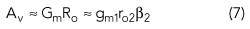
Through Equation 7, it can be shown that the maximum available voltage gain of a stacked pair is higher by a factor β2 than for the case of a single transistor. In addition, the stacked configuration helps to minimize the Miller effect and improves the isolation between the input and output of the amplifier.