
A Dynamic Drain Current Model for MESFET/HEMTs Valid Under Varying Static Bias and Temperature Conditions
J.M. Cairon, A. Tazon, T. Fernandez, C. Navarro and A. Mediavilla
University of Cantabria
Cantabria, Spain
J. Rodriguez-Tellez
University of Bradford
West Yorkshire, UK
Modifications to the Dortu-Muller DC drain current model for GaAs MESFET/HEMT devices that enable the dynamic output characteristics of the device to be simulated under different temperature and static bias conditions are presented. The modifications illustrate the difficulties in the simulation of the changes introduced into the device dynamic characteristics by frequency dispersion, thermal and electric field effects.
In this article the Dortu and Muller1 DC drain current model for the GaAs MESFET/HEMT device is modified to simulate the device dynamic output characteristics under different ambient temperatures and static bias conditions. This modified model enables, possibly for the first time, the circuit designer to simulate the device and hence circuit under these conditions. The model and modeling procedures presented can be implemented quickly and easily from purely terminal measurements and the model lends itself to implementation in CAD packages. The complexity of the model can also be easily reduced if, for example, the thermal or static bias range of interest is reduced.
MEASUREMENTS AND DEVICE CONSIDERED
In order to develop a dynamic model valid over a wide temperature and static bias range the following measurements were performed. For pulsed IV measurements, the dynamic characteristics of the device were measured using a pulsed measurement system2 over the dynamic range of vgs = 3 to 0 V and vds = 0 to 5 V. This dynamic bias range covers the entire region of normal operation for the device. In these measurements pulses 1 µs wide with a period of 1 ms and rise-and-fall-times of 50 ns were employed to switch the gate-source and drain-source terminals of the device. These pulse conditions have been shown to ensure that no self-heating takes place from the dynamic bias.3
Performing the pulsed IV measurements under different static bias conditions incorporated the effects of the static bias on the dynamic characteristics of the device. In this respect measurements were made at three VDS static points (5 V, 3 V and 0.5 V) and for each of these points, three VGS cases (0 V, 1.5 V and 3 V) were considered. The VDS = 0 V, VGS = 3 V static point where the device is pinched-off was also considered. These static points cover a wide region of operation.
The effects of ambient temperature on the behavior of the device were assessed by performing the described measurements at different ambient temperatures. The measurements were performed with a Peltier heating/cooling unit over the temperature range of 12° to +60°C. A thermocouple was placed directly over the device package to monitor the ambient temperature accurately. In the development of the model equations either the actual device temperature (ambient and self-heating temperature) or the ambient temperature can be used.
Since the described measurements are carried out at a signal frequency of 1 kHz, the resulting model represents the device IV behavior after the frequency dispersion effect has settled.4 For this device the frequency dispersion effect was most pronounced in the 60 to 700 Hz region. Beyond 700 Hz the frequency dispersion effect remained reasonably constant with increasing frequency.
To demonstrate the accuracy and flexibility of the model, a packaged power MESFET device from GEC-Marconi Materials Ltd. was employed as the test vehicle. The device selected comprised of 10 fingers each with a gate-width of 140 µm. This device has a 0.5 µm gate length and a pinch-off voltage of 3 V. At VGS = 0 V, VDS = 2 V the device carries a drain current in excess of 300 mA. The device was primarily chosen to illustrate more clearly the effects of the self-heating due to the static bias. The same measurements and modeling procedures have been applied successfully to other devices.
MODEL EMPLOYED FOR INITIAL INVESTIGATION
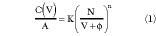
The model developed by Dortu and Muller was employed to represent the dynamic IV characteristics of the device. This is a DC IV model which is based on the work performed by Materka.5 This model has been shown to provide good accuracy in the linear and saturation regions under low and high current conditions.6 The model simulates the DC dependence of the drain current on the DC junction voltages as1
Although the Dortu model was primarily developed for representing the DC IV characteristics of the device, it was found to be accurate in representing the dynamic IV characteristics as well.
The procedure for determining which of the Dortu model parameters are important for representing the effects of temperature and static bias on the dynamic characteristics was as follows: All of the Dortu and Muller model parameters were extracted from the measured dynamic characteristics at one specific temperature and static bias point (Step 1). The extracted parameters were then optimized against the measured data until the best fit was obtained over the widest dynamic bias range (Step 2). These two steps were then repeated for the other temperature and static bias points.
This exercise yielded a family of model parameter values as a function of ambient temperature and static bias. The exercise revealed that for representing ambient temperature effects, parameters IDSS , VTO and KE were the most important. In this respect, these results are in keeping with the observed temperature dependence observed from a purely DC point of view.79 The effects of the static bias on the dynamic characteristics were more comprehensive and, in addition to the described three parameters, required  , SL , SS , KG and E to be included. Whereas the former three parameters were found to be important from a thermal and static bias point of view, the , SL , SS , KG and E parameters were mainly dependent on the static bias.
With this trend established, the following procedure was then applied to re-evaluate the model parameter values as a function of static bias and temperature. Using the IV characteristics of the device measured at 20°C and at VDS = 3 V, VGS = 1.5 V, all of the Dortu and Muller parameters were estimated and optimized. This static bias and temperature point was used as a reference point since it represents the conditions where the device and hence model are most likely to be employed.
Using the characteristics measured at the same static bias point, step one was repeated for each of the remaining characteristics measured at different ambient temperatures. For these cases, the parameter values used for , SS , SL , KG and E were those estimated in step one. This yielded the variation of IDSS , VTO and KE as a function of ambient temperature for the VDS = 3 V, VGS = 1.5 V static point. Clearly, because of the process employed, the most accurate set of parameter values correspond to the 20°C case since all of the model parameters were included in the optimization process.
Step one and two were then repeated for the other static bias points as a function of ambient temperature. This yielded the variation of IDSS , VTO and KE as a function of ambient temperature and static bias and the variation of the remaining parameters as a function of static bias with the temperature at 20°C as the reference point.
The selection of the reference temperature and static bias points, from where all of the parameters of the model have their origin, was found to be significant in determining the trend of the resulting optimized model data. The selection of the static bias point was, not surprisingly, found to be more important than the selection of the ambient temperature point. This result is due to the complex interaction between temperature and frequency dispersion effects, which is also electric field dependent. The temperature range and more importantly the static bias range over which the resulting model is to be valid, determines to a large extent the complexity of the expressions required to simulate the dependency of the model parameters on static bias and ambient temperature. Significant reductions in model complexity could, for example, be achieved if, from a static bias point of view, the static bias points corresponding to the linear region and the pinch-off point were not included. This elimination would, of course, render the model less useful to many applications.
EXPRESSIONS FOR MODELING AMBIENT TEMPERATURE EFFECTS
The results obtained from the previously described exercise, not surprisingly, indicates an almost linear dependency on ambient temperature for parameters IDSS , VTO and KE under all of the static bias conditions employed. Therefore, these parameters were simulated as
|
IDSS (T) |
= |
IDSSI (TT0 ) + IDS0 |
|
VT0 (T) |
= |
VT01 (TT0 ) + VT00 |
|
KE (T) |
= |
KE1 (TT0 ) + KE0 |
where
IDSO , VTOO , KEO = value of IDSS , VTO and KE at the reference ambient temperature
(20°C)
IDSS1 , VTO1 , KE1 = temperature coefficient
Clearly, these six parameters vary as the static bias point is varied since this change varies the self-heating effect. This effect changes the dynamic characteristics of the device for several reasons; first, because of the change in the device temperature and second because such a change influences the frequency dispersion effect. The change in the electric field as the static bias point is varied also changes the trapping states and this change also influences the dynamic characteristics. This interaction is quite difficult to simulate and since a physics based approach is not available empirical expressions are required. The following expressions10,11 were found to give a reasonable compromise between accuracy and execution speed
where
ß0 (VGS , VDS ) = ß00 + ß10 VGS
+ ß30 VGS 2 + ß20 VDS + ß40 VDS 2
and
ß1 (VGS , VDS ) = ß11 + ß01 VGS
+ VDS (ß21 VGS + ß31 VDS ).
Similarly for VT0 and KE
VT00 (VGS ,VDS ) = VT00 + VT10 VGS
+ VT20 VGS 3 + VT30 VDS 2
+ VT40 (VDS VGS )VT50
VT01 (VGS ,VDS ) = VT01 + VT11 VGS
+ VT31 VGS 2 + VT21 VDS
+ VT41 VDS 2 + VT51 (VDS VGS )VT61
KE0 (VGS ,VDS ) = KE00 + KE10 VGS
+ KE20 VGS 2 + KE30 VDS 2
+ KE40 (VDS 2 VGS )KE50
KE1 (VGS ,VDS ) = KE01 + KE11 VGS 3
+ KE21 VDS + (VDS VGS )KE31
As is to be expected, each of these parameters require at least a second order polynomial in VGS and VDS to describe the complex interaction between electric field and self-heating effects. An indication of this interaction and the quality of fit provided by these equations is shown graphically in Figures 1 to 3 at one ambient temperature point. Of the two effects represented by these parameters, the effect of the change in the electric field is the more important.


The definition of the complex nature of the frequency dispersion effect is, of course, not yet complete since parameters *, SL , SS , KG and E also must be modified to account for the effects of the static bias as
*(VGS ,VDS ) =
P1* + P2* VGS + P3* VDS + P4* VDS 2
SL (VGS ,VDS ) = P1SL + P2SL VGS
+ P3SL VDS + P4SL VDS 2
SS (VGS ,VDS ) = P1SS + P2SS VGS
+ P3SS VDS + P4SS VDS 2
KG (VGS ,VDS ) = P1KG + P2KG VGS
+ P3KG VDS + P4KG VDS 2
E(VGS ,VDS ) = P1E + P2E VGS
+ P3E VDS + P4E VDS 2
Note that while these parameters are effectively ambient temperature independent (and by implication, therefore, independent of self-heating), they do vary with the static bias and such variations have a significant effect on the model accuracy.
SIMULATION RESULTS
Using the previously modified Dortu and Muller model, the computed dynamic characteristics can be compared with the measured dynamic characteristics under a variety of static bias and ambient temperature conditions as shown in Figure 4 . From these diagrams, it can be seen that the model provides good accuracy over a broad temperature and static bias range. This quality of fit is not significantly degraded when the device is operating near the pinch-off point from a static or dynamic point of view.

From a computer processing point of view, the model is certainly slower than the conventional Dortu and Muller model (approximately three times slower) but is sufficiently fast to be useful for circuit design purposes. The additional features it offers offset the slower execution speed.
The application and accuracy of the model in conditions not considered in the parameter estimation process, but falling within the bias and temperature area considered, was found to be good. However, when the model was applied in a bias or temperature point falling outside of the area considered in the modeling process, poor accuracy and convergence difficulties were encountered. Of course, this shortcoming can be easily avoided by selecting appropriate conditions for the modeling exercise.
The scalability of the parameters of the model is a more difficult problem to solve, especially with the parameters that simulate second order effects. These parameters do not appear to follow any obvious rules as the gate-width or numbers of fingers of the device are varied. This problem arises almost entirely from the static bias variation rather than from the variation of the ambient temperature. It is believed this effect arises from the complex dependence of the frequency dispersion problem on the processing and device design. This is an issue which is currently under assessment.
CONCLUSION
In summary the following main points have emerged from the work presented in this article: Simple modifications carried out to the Dortu and Muller DC drain current model has led to a model capable of simulating the dynamic IV characteristics of the device under different temperature and static bias conditions. The model modifications and modeling procedures are simple to implement requiring only terminal measurements. The complexity of the model can be reduced if required and the generality of the approach enables the same idea to be implemented with other drain current expressions. Finally, the results presented illustrate quite clearly the significant and complex effect that the static bias has on the dynamic characteristics of the device. Although the self-heating effect is partly responsible for this effect it is the dependence of the frequency dispersion effect on electric field, which greatly increases the model complexity. *
References
1. J.M. Dortu and J.E. Muller, "Accurate Large-signal GaAs MEFET Modeling for Power MMIC Amplifier Design," 2nd International Workshop on Integrated Nonlinear Microwave and Millimeter Wave Circuits , Duisburg 1992.
2. T. Fernandez, Y. Newport, J.M. Zamarillo, A. Mediavilla and A Tazon, "High Speed Automated Pulsed IV Measurement System," 23rd European Microwave Conference , Madrid, September 1993, pp. 494496.
3. J. Rodriguez-Tellez, A. Mediavilla, T. Fernandez and A. Tazon, "A Method for Characterizing Frequency Dispersion and Thermal Effects Independently in GaAs FETs," European Microwave Conference, Munich, October 46 1999, pp. 399402.
4. J. Rodriguez-Tellez, B.P. Stothard and M. Al-Daas, "Static, Pulsed and Frequency-dependent IV Characteristics of GaAs FETs," IEE Proceedings , Pt G, Vol. 143, No. 3, June 1996, pp. 129133.
5. A. Materka and T. Kacprzak, "Computer Calculation of Large Signal GaAs FET Amplifier Characteristics," IEEE Transactions on Microwave Theory and Techniques , Vol. MTT-33, No. 2, February 1985.
6. J. Rodriguez-Tellez, M. Al-Daas and K.A. Mezher, "Comparison of Nonlinear MESFET Models for Wideband Circuit Design," IEEE Trans. ED , Vol. 41, No. 3, March 1994, pp. 288293.
7. R.E. Anholt and S.E. Swirthun, "Experimental Investigation of the Temperature Dependence of GaAs FET Equivalent Circuits", IEEE Trans. ED , Vol. 39, September 1992, pp. 20292036.
8. J. Rodriguez-Tellez and B.P. Stothard, "Simulation of Temperature and Bias Dependencies of ß and VTO of GaAs MESFET Devices," IEEE Trans. ED , Vol. 40, No. 10, October 1993, pp. 17301735.
9. L. Selvi and B. Ricco, "Modeling Temperature Effects in the DC-IV Characteristics of GaAs MESFETs," IEEE Trans. ED Vol. 40, February 1993, pp. 273277.
10. T. Fernandez, Y. Newport, J.M. Zanarillo, A. Tazon and A. Mediavilla, "Extracting a Bias-dependent Large Signal MESFET Model From Pulsed I/V Measurements", IEEE Transactions on Microwave Theory and Techniques , Vol. 44,No. 3, March 1996, pp. 372378.
11. A. Mediavilla, A. Tazon, J.L. Garcia, T. Fernandez, J.A. Garcia, C. Navarro and J.M. Zamanillo, "Dynamic Properties and Modeling of Large Signal, Thermal, Optical and Intermodulation Effects in Microwave GaAs Devices," 1977 IEEE MTT-S International Symposium , Denver, CO, June 813, 1997.