
Time Domain Analysis of a Printed Circuit Board Via
Brock J. LaMeres
Agilent Technologies
Colorado Springs, CO
T.S. Kalkur
University of Colorado, Department of Electrical and Computer Engineering
Colorado Springs, CO
This article describes the time domain analysis of a printed circuit board via connecting two semi-infinitely-long microstrip transmission lines above a ground plane. An equivalent circuit consisting of capacitance and inductance is given. Time domain reflectometry measurements are taken on an experimental printed circuit board containing vias of various geometries. The responses of the test vias are measured as the radii of the pad, cylinder and ground plane clearance are swept. The empirical data are then compared to previously taken simulation data and the differences are discussed.
Minimizing discontinuities in high speed controlled impedance transport systems is of considerable importance to the functionality of that system.1 Excess capacitance and inductance on a transmission line can lead to reflections, signal speed degradation and unexpected switching in digital circuits. One such discontinuity that is common in multilayered printed circuit boards is the via. The accurate characterization of a printed circuit board via is an important issue in the successful design of high speed circuits implemented on multilayered printed circuit boards. Theoretical analysis of the via connecting the microstrips has been studied in detail by many investigators.2?4
A printed circuit board via is a structure that connects two transmission lines on different layers of a multilayered printed circuit board. A via consists of a hole drilled through a printed circuit board and plated with a conducting material. (This plated hole is referred to as the cylinder in this article.) On each layer on which a transmission line is connected to the cylinder, a circular pad of conducting material is placed about the cylinder. These pads provide contacts for the transmission lines. In most high speed circuit boards, the cylinder of the via passes through at least one ground plane. A clearance hole in the ground plane is left so that the cylinder can pass without making contact. Figure 1 shows a three-dimensional cross section of two microstrip transmission lines that connect to a via that passes through one ground plane. The three parameters that this article investigates are marked on the diagram. The parameters are the radii of the pad, cylinder and ground clearance.

The electrical model of a via can be broken into three sections: the upper pad, cylinder and lower pad. Each section consists of a capacitance and inductance. This article investigates the impact of the physical geometry of a via and its effect on signal integrity as signals propagate through it. The degradation of signal integrity is a result of parasitic excess capacitance and inductance. The term excess refers to any additional capacitance or inductance that results in a via's characteristic impedance not matching the characteristic impedance of the connecting transmission lines. The investigation is limited to the connection of microstrip transmission lines to the via. The effect on the characteristic impedance of the via is studied as its physical geometry is altered. Specifically, time domain reflectometer (TDR) measurements are taken as the radii of the pad, cylinder and ground backoff are varied on a set of experimental vias.
TIME DOMAIN REFLECTOMETRY
A TDR is a device that sends a step-shaped pulse down a transmission line and concurrently measures the reflected waveform. By monitoring the incident and reflected waves, the TDR is able to determine the characteristic impedance of any point on the line. The measurement is performed in the time domain so discontinuities can be isolated from each other with respect to time.
The goal of a transmission line transport system is to deliver an electrical signal to a specific point without the addition of any distortion or dispersion to that signal. As long as the characteristic impedance, Zo , of the transmission line is constant at every point throughout the length of the line, the signal will be delivered in tact. When areas of a transmission line have a different Zo than the rest of the line, reflections will occur. The measure of how much of the incident signal is reflected is defined as G (reflection coefficient). G is defined as5

In this expression, Zo is the characteristic impedance of the transmission line that is used to transmit the signal. ZL is the impedance of the load to where the signal is being delivered (or the impedance of the element immediately in front of the signal). The expression for the amount of the signal that is reflected is defined as5
VREFLECTED = G VINCIDENT (2)
This expression illustrates that when the impedance of the load matches the impedance of the transport system, G will be zero and the entire signal will be delivered. This article only considers lossless transmission lines. For a lossless transmission line, the characteristic impedance is defined as6

Any capacitance or inductance that results in an area of mismatched impedance is considered excess.
Using time domain reflectometry, regions of mismatched impedance on a transmission line can be observed due to their reflection of the incident signal. The instrument used to accomplish this task is an Agilent 54750 digitizing oscilloscope with an Agilent 54754A differential TDR modular plug-in.
EQUIVALENT CIRCUIT
To fully characterize the electrical response of a via, an equivalent circuit must be developed. The circuit must be able to accurately model the response while still being practical enough to be used in a development process. The complexity of the equivalent circuit can be reduced by limiting the bandwidth over which the equivalent circuit is accurate.
By using knowledge of the via's response, a circuit can be developed that accurately models the effect of the three segments of the via. The total response of the via at lower frequencies tends to look capacitive, or low impedance. As frequency increases, the effect of each segment becomes more distinct. When this occurs, the first and third sections (pads) will continue to look capacitive, but the second section (cylinder) will tend to look more inductive (or higher impedance) as the cylinder diameter is reduced. The equivalent circuit, shown in Figure 2 , portrays this behavior. As demonstrated in earlier investigations,4 this circuit is able to model the response of a via up to 100 ps rise times.
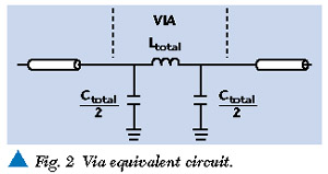
Using the approximation that the rise-time bandwidth product is equal to 0.35 (tr × BW = 0.35), a 100 ps rise time will correspond to a bandwidth of approximately 3.5 GHz. The TDR measurements use a 100 ps rise-time step pulse. The 100 ps rise time covers most signal rise times seen today in high speed digital circuits implemented on printed circuit boards.
TIME DOMAIN ANALYSIS
This section examines the time domain measurements taken on a test printed circuit board containing vias of varying geometries. The circuit board was designed to show the empirical effect of the via's physical geometry on its electrical response. The time domain analysis is accomplished by using time domain reflectometry.6 Figure 3 shows the equivalent circuit of the TDR and test printed circuit board experimental setup. The TDR oscilloscope has an output impedance of 50 W . In order to show the discontinuity caused by the via in more detail, the test printed circuit board uses 75 W microstrip transmission lines. Since the TDR measurement gives the ability to separate discontinuities as a function of time, this mismatch does not affect the measurement. The experimental setup uses the previously presented equivalent circuit to model the via.

Figure 4 shows the test printed circuit board developed to examine the empirical results of the electrical response of various via sizes. Figure 5 shows the laboratory setup used to take the TDR measurements. The test printed circuit board has 15 vias that are used in this experiment. Five vias are used in each of the pad radius, cylinder radius and ground clearance radius parametric sweeps.


Figure 6 shows the first set of measurements where the pad radius is varied. It can be seen that the impedance of the via decreases as the pad radius increases. The main factor contributing to this result is the increase in capacitance due to the increase in surface area of the via. Since capacitance is proportional to the surface area of the conductors and Equation 3 shows that Zo is inversely proportional to the capacitance, a larger pad will result in a region of lower impedance. Clearly it is more desirable to have a smaller pad. The limit on the minimum pad size that can be used is often dictated by the printed circuit board manufacturer.

Figure 7 shows the second set of measurements taken while varying the cylinder radius. Again it is shown that the impedance of the via decreases as the cylinder radius increases. This result is due to two factors. First, as in the previous measurement, the capacitance is increasing due to the increase in surface area of the conductors. Second, the cross-sectional area that the current flows through increases, thus decreasing the resistance and inductance that the signal sees. Since Zo is proportional to inductance, this condition along with the increase in capacitance will lead to a region of lower impedance. It is clearly more desirable to have as small a cylinder radius as possible. This specification is limited by the minimum drill bit radius that the printed circuit board manufacturer has available.

Figure 8 shows the last set of measurements taken while varying the ground plane clearance radius. Here it is shown that the impedance increases as the ground plane radius increases. This impedance increase is due to a decrease in the capacitance. Since capacitance is inversely proportional to the distance between the two conductors, a decrease in capacitance leads to a region of higher impedance.

Figures 9 , 10 and 11 show the empirical TDR data compared to simulation data to examine the accuracy of the equivalent circuit. The simulations use a three-dimensional electromagnetic simulator to extract the electrical parameters C and L for a specific via geometry. These values are then inserted into a SPICE simulation of the experimental TDR setup. One via from each of the three parametric sweeps on the test printed circuit board is compared to the corresponding simulation data.


CONCLUSION
This article presented an equivalent circuit for the characterization of a printed circuit board via as well as the results of time domain reflectometry measurements taken on a test printed circuit board containing vias whose geometries were swept. The empirical data were compared to simulation results of the equivalent circuit in the experimental setup. It was demonstrated that an increase in the radius of the pad and cylinder of the via results in a decrease in characteristic impedance. It was also shown that an increase in the ground clearance radius results in an increase in characteristic impedance.
When designing high speed transport systems implemented on printed circuit boards, signal integrity is of great importance. Discontinuities can lead to reflections and signal rise-time degradation, and may cause unexpected switching in digital systems. A common source of discontinuity in multilayered printed circuit boards is when a transmission line changes signal layers using a via. When designing a high speed system, all sources of discontinuities must be modeled to account for their negative effects. By accurately modeling the printed circuit board via and knowing what physical dimensions affect its electrical response, a designer can counter its parasitic effects. This article has presented an accurate model for the printed circuit board via that can be used in a development process. By considering how the physical dimensions of a via affect signal integrity, the negative effect of the via can be minimized.
ACKNOWLEDGMENT
The authors are grateful to Agilent Technologies and Hudco for their support of this work.
References
1. Glenn R. Blackwell (editor), Circuit Boards, The Electronic Packaging Handbook , CRC Press, 1999.
2. T. Wang, R.F. Harrington and J.R. Mautz, "The Equivalent Circuit of a Via," IEEE Trans. Soc. of Comput. Simulation , Vol. 4, April 1987, pp. 97?123.
3. T. Wang, R.F. Harrington and J.R. Mautz, "Quasi-static Analysis of a Microstrip Via through a Hole in a Ground Plane," IEEE Transactions on Microwave Theory and Techniques , Vol. MTT-36, June 1988, pp. 1008?1013.
4. B.J. LaMeres, "Characterization of a Printed Circuit Board Via," Master's Thesis, University of Colorado, Colorado Springs, CO, May 30, 2000.
5. Fawwaz T. Ulaby, Fundamentals of Applied Electromagnetics , Prentice Hall, NJ, 1997.
6. D. Dascher, "Measuring Parasitic Capacitance and Inductance Using TDR," Hewlett-Packard Journal , April 1996, pp. 8396.
 Brock J. LaMeres received his BSEE degree from Montana State University in 1998 and is currently working on his MSEE at the University of Colorado. As an undergraduate he conducted research in alternative energy and intelligent control systems. He also interned for VeriBest Inc., an EDA development company, and Micron Technology, a semiconductor development company. In 1999, LaMeres joined Agilent Technologies as a hardware design engineer where he develops semiconductor test equipment.
 Thottam S. Kalkur received his BSc degree from the University of Mysore in 1973, his MS degree from the Indian Institute of Science, Bangalore, in 1979 and his PhD from the University of Western Australia in 1986. From 1975 to 1977, he was a lecturer at St. Agnes College, Mangalore. From 1979 to 1982, he was an assistant executive engineer at Indian Telephone Industries, Bangalore. In 1985, Kalkur joined the faculty of the department of electrical and computer engineering at the University of Colorado, Colorado Springs, where he is presently a professor.