
A Simple Gain Equalizer for a PCS-band Amplifier
Barney Arntz
Philips Semiconductors
Mansfield, MA
A simple distributed network is described, which has the effect of flattening the frequency response of an amplifier or system by reducing its gain in a particular frequency range. Operating with a quarter-wave line coupler (which can be printed on the circuit board), the equalizer acts as a very shallow notch filter with controlled bandwidth.
Microwave power amplifiers with operating bandwidths that are a few percent of their center frequency, similar to those used in today's cellular and PCS base stations, achieve efficiency with tuned networks on the inputs and outputs of the power devices. These networks are intended to negate, in part, the unavoidable parasitics of the device and packaging. The power devices themselves have impedances with an imaginary (reactive) part that is on the same order of magnitude as their real (resistive) part, making a tuned circuit a better choice than a wideband (decade or more) design when only operating over a narrow band.
BANDWIDTH ISSUES IN POWER AMPLIFIERS
A byproduct of a tuned design is that the gain rolls off at the edges of the intended frequency range. Even in low Q designs, there is often 0.2 to 0.5 dB of gain rolloff at the band edges. This characteristic is aggravated in cascaded designs, which often contain hybrid couplers, isolators and other devices that have gain rolloff at the edges. This rolloff becomes especially important in the loops of feedforward amplifiers, whose cancellation of distortion or carrier signals depends on gain flatness.
THE EQUALIZER CIRCUIT
The circuit described is a tuned network with a slight loss at the center band and minimal loss at the band edges. The amount of gain reduction and Q is adjustable, as well as the center frequency. This circuit operates at 50 O as implemented and can be used to compensate for a single stage or several stages of gain. The phase linearity and delay flatness are not degraded.
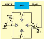
The schematic of the gain equalizer is shown in Figure 1 . The coupled line appears slightly longer than a quarter-wave so that the resonant frequency can be adjusted with C1. On a Smith chart, the top of the capacitor (without the remainder of the circuit) presents an impedance that is totally reflective (that is, on the outside of the circle) at approximately 120°. The addition of the line brings the impedance at the junction of R1 around the chart by twice the line length, or 240°, to an open (0°). The frequency at which the open occurs is the resonant point of the circuit and can be adjusted approximately ±10 percent without difficulty. The adjustability of the center frequency can be used to take up tolerances in the circuit board etching and line lengths.

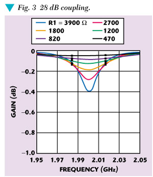
R1 controls the depth of the notch, as shown by simulation in Figure 2 . The coupling value, which is in the general range of 18 to 30 dB, controls the Q, or width of the notch, as can be seen by comparing the simulation data for 28 dB coupling, shown in Figure 3 , with the previous graph of 20 dB coupling. Actually, R1 and the coupling value interact, and both parameters control the depth and Q of the notch, but in different ways. To the extent that the coupling value is not directly controllable in printed designs once the unit is manufactured, this fixed coupling can be somewhat compensated for by adjusting R1, which affects the depth of the notch as well. Thus, in practice, the coupling value is not critical. There are enough degrees of freedom to equalize a wide range of circuits having a generally soft bandpass characteristic.
RETURN LOSS
There is necessarily some reflection at the input from this design. The calculated return loss of the circuit is shown in Figure 4 . Working to advantage in keeping S11 reasonably controlled is the fact that, for a given amount of coupling, the error voltage that reflects back to the input is down by twice that coupling. For example, for a 20 dB coupler, the return trip from the input, through the coupler and back to the input has a loss of 40 dB. This return loss keeps the resonant circuit's effect on the main line to a minimum. To achieve a gain dip of 0.5 dB, the main path voltage must be pulled down by only 5.9 percent.

Figure 5 shows measurements on a single stage of amplification with and without compensation. The gain block is a 45 W laterally diffused metal-oxide semiconductor device with printed matching networks on the input and output. The gain flatness without compensation is 0.2 dB across 90 MHz at a center frequency of 1960 MHz. With compensation, the gain flatness is 0.08 dB. To achieve this gain flatness, approximately 0.35 dB of overall gain was sacrificed.

PHASE LINEARITY
When adding a frequency-dependent linear network in feedforward and/or pulsed applications, the phase linearity must be checked to see that it has not been corrupted. Figure 6 shows the calculated phase linearity of the gain stage with and without compensation. A phase offset has been applied between the curves for plotting purposes so that the scale can be expanded. In addition, the electrical delay was subtracted out. It can be seen that the phase linearity has not been degraded. Similarly, the delay flatness (not shown) has not been degraded. The group delay has been reduced by a small amount (approximately 70 ps).

CONCLUSION
A simple printed circuit gain equalizer circuit has been described, which comprises a quarter-wave line coupler, variable capacitance and selected resistor. The network is capable of flattening the gain of narrowband power amplifiers used in today's cellular and PCS base stations. *