
ADS CIRCUIT MODEL
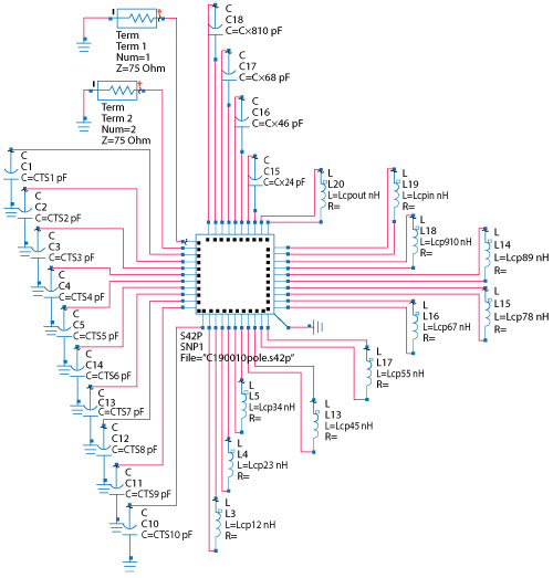
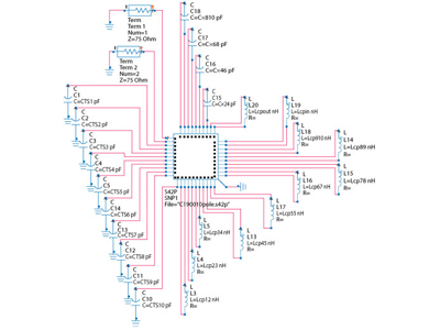
Figure 5 ADS circuit model of the 10 pole combline filter.
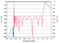
Figure 6 ADS optimized ideal result for the filter topology shown in Figure 3, with two added lumped LC highpass sections in front of the first and the last resonator.
An ADS model corresponding to the topology diagram in Figure 3 is shown in Figure 5. The large box in the center of the diagram is the 42-port S-matrix, which contains the data previously calculated in HFSS. Each terminal in the box corresponds to a port in the HFSS model. The 10 capacitors shown to the lower left in the figure represent the tuning screws. The two coaxial I/O ports are placed at the upper left corner. The rest of the components represent the couplings in the filter. In general, the mainline couplings are implemented as lumped inductors, x-couplings as capacitors and corrections to the tuning screw penetrations in the resonators also as capacitors. All the lumped components shown are subject to optimization.
With the circuit model defined, the task is to optimize all the lumped components until the characteristic in Figure 1 is obtained as close as possible. Unfortunately, it turns out that this cannot be achieved with the described ADS model: the two coupling inductors Lcpin and Lcpout (see Figure 3), which connect the first and last resonators to the I/O connectors, reach their lower limits of 0 nH.
The problem is that stronger couplings are needed than can be realized. From Table 2, it is seen that these couplings (S1 and L10) are, by far, the strongest couplings in the filter; however, the coupling values decrease toward the center of the filter. This problem is solved by adding two lumped LC highpass sections outside the mechanical 10-pole filter. The strongest couplings are shifted from the outermost combline resonators to the pair of lumped LC filters, where strong couplings are easier to realize. Adding the two lumped LC sections increases the overall insertion loss a bit, since their unloaded Qs may be 10x lower than the combline resonators. The lumped highpass sections are mounted on the printed circuit board’s (PCB) connection with the combline filter. Two LC sections are easily added to the ADS model between the two 75 Ω ports and the 42 port S-block. The optimization now succeeds with the results shown in Figure 6.
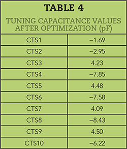
In the HFSS model, all tuning screws penetrate the resonator center holes with approximately 13 mm overlap. The values of the tuning screw lumped capacitances (CTS1 to CTS10 in Figure 5) are corrections to the capacitances of the tuning screws in these positions. The design strategy is first to vary the diameter of the resonator top disk in the HFSS model until the tuning capacitances (CTS1 to CTS10 in Figure 5) are close to zero. A zero value means that the corresponding resonator is tuned correctly with a 13 mm tuning screw depth. The tuning capacitance values obtained after optimization are shown in Table 4. A negative value means that the resonator needs less capacitance and therefore a smaller top disk, while a positive value indicates the need for more capacitance and a larger disk.
With the new capacitance values, the top disk diameters in the HFSS model are changed, a new HFSS simulation is performed, followed by ADS optimization. The new CTS values are interpolated linearly to obtain a new set of diameters. The cycle is repeated until CTS values are so small that the differences can be absorbed by the tuning screws. The final resonator geometries are found by running the HFSS model a few times. Each HFSS simulation took approximately two hours on our system, and the corresponding ADS optimization took between 45 and 60 minutes. It is clear that such a filter could never be optimized using HFSS alone, where many hundreds of iterations would be required.
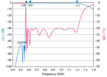
Figure 7 Resulting ADS/HFSS filter characteristic, including losses.
FINAL HFSS MODEL
The characteristic obtained by the final ADS/HFSS model is shown in Figure 7.
In this model, we have:
- Changed the resonator top disk diameters until the lumped tuning capacitance values (CTS) are around 0 pF.
- Modified the tuning screw penetrations to keep the number of different resonator geometries minimum. This resulted in only four different resonator geometries, keeping the cost of manufacturing to a minimum.
- Replaced the inductive mainline couplings with standard inductance values. These inductors are represented by S-parameter models as provided by the manufacturer (Coilcraft). The inductance values range from 8 to 35 nH.
- Not assigned standard values to the x-coupling capacitors since these are represented by variable SMD capacitors.
- Included losses in both the cavity combline filter and in the lumped coupling network. The latter includes an approximately 100 mm FR4 transmission line in the main signal path.
During the optimization process, the order in which the x-couplings ended up being placed in the filter may have changed compared to the initial order indicated in Table 2. This was not controlled, since all four x-couplings had similar coupling bandwidths.
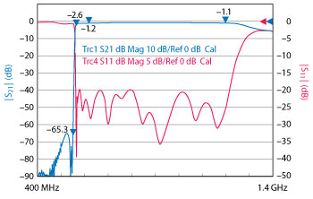
Figure 8 Measured filter characteristic of manufactured filter.
PHYSICAL FILTER
The filter designed in the previous sections was manufactured, assembled and tuned, achieving the result shown in Figure 8. Comparing the model characteristic in Figure 7, very good agreement was obtained between measured and simulated characteristics. The measured characteristic includes losses from two short coax cables (0.4 dB in total), which are not present in the model.
Some modifications were made to some of the lumped coupling inductor values (Lcp) to arrive at the performance in Figure 8. The reason that deviations from model values were necessary is believed to originate from the difference in the way the lumped ports are defined in the model and how the inductor tap points are realized in practice. All lumped couplings are mounted on a single FR4 PCB, as shown in the photo of the final filter in Figure 9. This PCB is attached to the underside of the resonator top disks with SMD spacer tubes and screws; in the model, the inductors are tapped directly to the topside of the disks.
The two lumped highpass PCB sections at the I/O are visible in Figure 9 along the lower edge of the filter. The four lumped trimmer SMD capacitors used in the x-coupling network are visible along the horizontal middle of the filter.
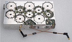
Figure 9 Manufactured filter without lid, showing coupling PCB, mushroom resonators, filter body and coaxial I/O lines.
CONCLUSION
This article describes the design and development of a compact, ultra-wideband, coaxial cavity, combline “brick wall” filter covering 564 to 1200 MHz. Normally, combline filters are used for relative bandwidths up to approximately 15 percent. In this work, the filter has more than 70 percent relative bandwidth, achieved using a combination of 3D EM simulation techniques and circuit simulation. For design, we used a combination of CMS and circuit simulation (ADS); for the 3D EM solver, we used HFSS.
Even though combline filters and CMS are normally not suitable for wideband applications, accurate results were achieved through co-simulation, even though this design was far outside the “comfort zone” for both filter type and synthesis tool.
The filter designed and manufactured in this work is a 10-pole, combline, cavity filter with mushroom-shaped resonators. All couplings were made with lumped components (inductors and capacitors) tapped to the top disk of the resonators. Four x-couplings were used to achieve the “brick wall” characteristic on the low-band side of the filter. A 42-port scattering matrix generated by HFSS was used to represent the mechanical part of the filter, for optimization in the circuit simulator. Excellent agreement was observed between measurement and simulation.n
References
- D. G. Swanson and R. J. Wenzel, “Fast Analysis and Optimization of Combline Filters Using FEM,” IEEE MTT-S International Microwave Symposium Digest, May 2001, pp. 1159–1162.
- “CMS Software: Filter and Coupling Matrix Synthesis,” Guided Wave Technology, www.gwtsoft.com.
- M. Hagensen, “Narrowband Microwave Bandpass Filter Design by Coupling Matrix Synthesis,” Microwave Journal, Vol. 53, No. 4, April 2010, pp. 218–226.
- S. Shin and S. Kanamaluru, “Diplexer Design Using EM and Circuit Simulation Techniques,” IEEE Microwave Magazine, Vol. 8, No. 2, April 2007, pp. 77–82.
- M. Hagensen and A. Edquist, “Simplified Power Handling of Microwave Filters,” Microwave Journal, Vol. 55, No. 9, September 2012, pp 130–139.
- “Ansys HFSS,” Ansys, www.ansys.com/Products/Electronics/ANSYS-HFSS.
- “Advanced Design System (ADS),” Keysight Technologies, www.keysight.com/en/pc-1297113/advanced-design-system-ads.