
Distortions in Cascaded MMIC Power Amplifiers
Oleksandr Gorbachov and Yie-Der Shen
Hexawave Inc.
Hsinchu, Taiwan, R.O.C.
Many methods exist for the linearization of RF/microwave PAs.1?4 In most cases, these methods are applicable to high power amplifiers taking into account their cost, size, weight and power consumption. For low- and mid-power portable PAs, these issues can play a decisive role in the choice of the required circuit. Thus, PA circuit-level linearization techniques may be more attractive to achieve low distortion characteristics. 3,5-7 It is known that the main source of IMD in a PA is typically the cubic term of the PA transfer characteristic. These distortions may be compensated for by utilizing a second harmonic adjustment.3,4,8 This goal may be quite easily achieved with discrete components. However, purchased MMIC utilization complicates the task. This article describes a simple way to adjust distortions in a set of cascaded MMIC PAs.
PHASE-DELAYED INTERSTAGE ADJUSTMENT
Figure 1 shows the interstage circuit between cascaded MMIC FET PAs. The only transmission line length in the circuit may be adjusted. It is known4 that the PA output signal spectral purity may be improved by careful adjustment of the gain and phase shift of the second harmonic path. For maximum improvement, the power required for the second harmonic should be high enough (7 dB below that of the fundamental in the example4 ). It is also known that the series source inductance can decrease IMD in the PA and simultaneously facilitate a low noise amplifier (LNA) input and noise matching condition8 with increased in-band stability. Taking these issues into account, it can be concluded that a drive MMIC PA with bad linearity must be utilized and the line length adjusted to achieve the best total distortion characteristics of the complete MMIC set. The power produced by the final stage of the drive PA and the gain of the first stage of the second PA should have sufficient values to achieve this performance.

MEASUREMENT RESULTS
Measurements have been performed for a set of 3.5 GHz GaAs MESFET MMIC PAs to evaluate how much improvement of distortion characteristics may be achieved. The series feedback source inductance in both stages may be varied due to the non-via chip structures used.
First, the minimum possible inductance values were chosen. Figure 2 shows the two-tone extreme intermodulation characteristics resulting from adjustment of the line length over a wide margin. The difference in the line length between extreme values corresponds to a quarter-wavelength at the second harmonic. Accordingly, the amplifier's small-signal, single-tone gain is 42 dB at P1dB = 28.8 dBm and 40.7 dB at P1dB = 29.7 dB. The drain bias voltage is 7 V DC.

Next, both series inductances were increased by two to three times. Both drive and power MMIC PA stages were tuned for the highest linearity by operating as separate stages and tested using wideband 50
© input and output transmission lines. These two stages are combined through the variable-length transmission line, and the extreme values of the two-tone gain and IMD for the complete set are shown in Figure 3. Again, the line length corresponds to a quarter-wavelength at the second harmonic. The single-tone P1dB values are equal to 30.7 dBm for both cases. The input return loss values are better than 14 dB for both stages.
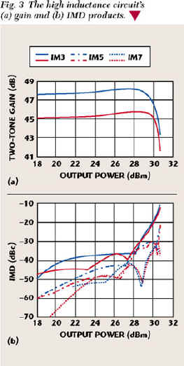
A great difference in characteristics is observed in the two data plots. In the first case, the variation of IMD products is quite small through the entire range of output power. Only a small difference can be observed for high power levels. However, it can be explained by an improvement of matching conditions for the input port of the power stage elevating P1dB. (As a reference, the input return loss value is 5 to 6 dB.) In the second case, the variation of IMD products is perceptibly high at mid-power levels with clearly observed sweet spots.6,7 At power levels close to P1dB and at the saturation region, the variation noted is very small. At some power levels, the IMD product difference reaches 5 to 7 dB. It should be noted that the circuits have different bias conditions. For both cases, the gate voltages were adjusted to achieve a maximum P1dB value.
Mid-power levels are important for operating within digitally modulated communication standards. Figure 4 shows the calculated results of ACPR10 for the 4.096 Mchips wideband CDMA standard. Calculations have been carried out taking into account only the IM3 (solid line) and IM3 + IM5 (dashed line) influence. The statistical drive signal has a logarithmic-normal distribution with a 2 dBm RMS power value (a close approximation of a one-user channel). A 2.5 dB improvement in ACPR value is observed through a wide range of output powers. This value corresponds completely to the gain difference between the extreme cases. For case 1, the analysis does not show any difference in ACPR value with the same output power back off. Comparing case 1 and case 2, a larger difference between adjacent IMD products for case 2 and more perceptible sweet spots due to the frequency-dependent negative feedback circuit (out-of-band harmonic termination adjustment6,11 ) are observed.

The drive stage for the set in case 2 was substituted for the low inductance stage for the set in case 1 (with less linearity). Improvements of 2 to 3 dB for IM3 and 5 to 7 dB for IM5 and IM7 were achieved at wide enough power levels close to saturation. Thus, the proposed MMIC set has perceptibly improved the distortion characteristics and spectral purity for CDMA signals without any additional filtering and amplifying stages for the second harmonic.4 Note that no attempt was made to reach the highest linearity by adjusting the input and output matching networks. The operation of the complete set is similar to using predistortion.1 By using this approach, it was determined that the first stage of a power MMIC should have fairly low gain to achieve better results. This fact is in contrast to commonly used design rules when the first stage of a multistage PA is usually tuned for high gain.
CONCLUSION
The method of adjustment of the second harmonic phase delay between two cascaded MMIC PA stages has been investigated. It was shown that the choice of a drive stage with bad linearity and a simple inductive feedback circuit at the input of the power stage allows the complete amplifier set to have an ACPR improved by 2 to 3 dB through a wide range of the output power for digitally modulated signals. This approach can be used for portable low cost circuits in different wireless communication systems. *
References
1. A. Katz, "SSPA Linearization," Microwave Journal, Vol. 42, No. 4, April 1999, pp. 22?44.
2. S. Andreoli, H.G. McClure, P. Banelli and S. Cacopardi, "Digital Linearizer for RF Amplifiers," IEEE Transactions on Broadcasting, Vol. 43, March 1997, pp. 12?19.
3. M.R. Moazzam and C.S. Aitchison, "A Low Third Order Intermodulation Amplifier with Harmonic Feedback Circuitry," 1996 IEEE MTT-S International Microwave Symposium Digest, June 1996, pp. 827?830.
4. D. Jing, W.S. Chan, S.M. Li and C.W. Li, "New Linearization Method Using Interstage Second Harmonic Enhancement," IEEE Transactions on Microwave and Guided Wave Letters, Vol. 8, No. 11, November 1998, pp. 402?404.
5. T. Iwai, S. Ohara, H. Yamada, Y. Yamaguchi, K. Imanishi and K. Joshin, "High Efficiency and High Linearity InGaP/ GaAs HBT Power Amplifiers: Matching Techniques of Source and Load Impedance to Improve Phase Distortion and Linearity," IEEE Transactions on Electron Devices, Vol. 45, No. 6, June 1998, pp. 1196?1200.
6. N.B. de Carvalho and J.C. Pedro, "Large Signal IMD Sweet Spots in Microwave Power Amplifiers," 1999 IEEE MTT-S International Microwave Symposium Digest, June 1999, Vol. 2, pp. 517?520.
7. J.A. Higgins and R.L. Kuvas, "Analysis and Improvement of Intermodulation Distortions in GaAs Power FETs," IEEE Transactions on Microwave Theory and Techniques, Vol. 28, No. 1, January 1980, pp. 9?17.
8. S.A. Maas, Nonlinear Microwave Circuits, Artech House, Norwood, MA, 1988.
9. Using the ATF-10236 in Low Noise Amplifier Applications in the UHF through 1.7 GHz Frequency Range, HP Application Note 1076.
10. O. Gorbachov, "IMD Products and Spectral Regrowth in CDMA Power Amplifiers," Microwave Journal, March 2000, Vol. 43, No. 3, pp. 96?108.
11. V. Aparin and C. Persico, "Effect of Out-of-band Terminations on Intermodulation Distortion in Common-emitter Circuits," 1999 IEEE MTT-S International Microwave Symposium Digest, June 1999, Vol. 3, pp. 977?980.
Oleksandr Gorbachov received his PhD degree in electrical engineering from Kiev Polytechnic Institute in 1990. Currently, he is employed by Gatax Technology Co., Nei-Hu, Taipei, Taiwan, R.O.C.
Yie-Der Shen received his PhD degree in electrical engineering from Stanford University. Currently, he is VP at Hexawave Inc., Hsinchu, Taiwan, R.O.C.