
RF Digital Attenuators in Plastic MLP Packages
M/A-COM
Lowell, MA
Broadband digital attenuators have been used to set power levels in RF and microwave circuits for many years. The concept is to electronically switch resistive T and P networks to attenuate and control signals. In doing so, attenuators must have low insertion loss, generate accurate (flat with frequency) attenuation levels, maintain low input and output SWR for all attenuation levels, produce low spurious signals, consume low DC power and switch very quickly. Although the basic "switched pad" circuits are well known and very useful, recent developments in GaAs MMICs and plastic packaging technologies have expanded operating frequencies while reducing physical size and costs.
Using this GaAs MMIC base, a family of digital attenuators producing five- and six-bit formats with least significant bit (LSB) weights of 0.5 and 1 dB have been developed in various package platforms. Initially, the product line consisted of multichip GaAs MMICs and silicon-based CMOS application-specific IC (ASIC) drivers packaged in ceramic flatpacks. For example, the model AT-263 attenuator utilizes a five-bit, 1 dB LSB MMIC in the RF path and two quad drivers to perform the interface for the TTL control signals. Its sister component, the model AT-283, has the same structure except the MMIC has a 0.5 dB LSB. The six-bit attenuators (models AT-106 and AT-107) employ five-bit MMICs with an additional dual-bit 16 dB MMIC connected in series to create the sixth bit. The 16 dB MMIC can be wirebond configured to produce a most significant bit (MSB) of 16 or 32 dB as the application requires. Figure 1 shows the interior views of five- and six-bit ceramic attenuators. For reference, the AT-106 attenuator with its four semiconductor chips occupies a total package area (body and leads) of 0.450" x 0.650" (11.4 x 16.5 mm).

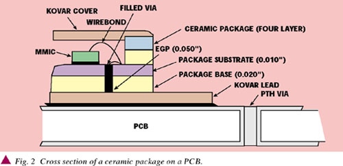
Two important aspects for high frequency performance are maintaining the impedance match for series (I/O) ports and minimizing the shunt (GND) inductance. Unless the MMIC designer specifically knows the final package in which the MMIC will be placed, MMICs are designed as stand-alone components. That is, the I/O ports are designed to look into 50 W networks while the die's base and the substrate it sits on should be a low inductance to ground. For example, Figure 2 shows the cross-sectional view of the effective ground path (EGP) for the MMIC in a ceramic package. This path effectively begins at the end wirebond and ends at the PCB ground. Ceramic packages, with their electrically grounded base and short EGP lengths, produce excellent RF performance up to 2.5 GHz. However, these packages have higher costs compared with plastic small outline integrated circuit (SOIC) devices, and that has resulted in limited demand in high volume, low cost applications.
To pursue the low cost attenuator market, the family of attenuators was expanded to include SOW-16 and 24-lead plastic packages. The AT65 series attenuators have reduced costs compared to the ceramic attenuators. However, the downside of transitioning to plastic packages was an increase in insertion loss and SWR. The additional lead inductance reduced the upper frequency limit to 2 GHz. The 0.300"-wide SOW package has an EGP that is approximately three times that of the ceramic (0.143" vs. 0.500"), as shown in Figure 3. While the SOIC plastic packages are perfectly acceptable for today's GSM and PCS telecommunication systems, they cannot support tomorrow's higher frequency applications or denser packaging objectives.

PACKAGE SELECTION
To realize a low cost plastic attenuator for frequencies beyond 2 GHz, the miniature leadless package (MLP) offered by various package vendors was investigated. This package platform offers low inductance I/O pads on a 0.5-mm pitch. In addition, an exposed conductive center die paddle provides improved RF grounding, which permits operation at higher frequencies. Aside from the size reduction, the package's main feature is that its cost is only slightly higher than that of the plastic SOIC packages. Figure 4 shows the ceramic, plastic SOW and MLP packages of the digital attenuator family.

The MLP package, with its ability to have the leadframe and paddle soldered directly to the PCB, can produce an EGP that is 82 percent shorter than that found in the referenced ceramic package. As shown in Figure 5, the EGP is limited to the thickness of the 0.008" copper leadframe. The outline for the 6.0 x 4.0 mm MLP package is shown in Figure 6.


DIE DEVELOPMENT
Once the package format was selected, developing ASICs and MMICs to accommodate the MLP platform became the next step. With typical package footprints at 10 to 30 percent of the SOIC packages, a total die shrink for all internal components was in order. The two drivers had to be combined into a single hex driver, and the single six-bit MMICs had to be developed to replace the two MMICs in the six-bit attenuators. Because new MMICs were required, it was determined that they should be designed to support much higher frequencies than the previous devices. For this effort, the upper frequency goal was increased to 4 GHz. This range would produce a respectable margin to ensure that the MLP attenuators would operate to a minimum of 3 GHz.
ASIC DRIVER
The MLP design effort began with the development of the hex channel ASIC driver, which meant increasing the number of channels while reducing the die size. Adding two driver channels was not an issue; however, reducing the size of the die to the required area meant minimizing output drive capability. Specifications were reduced from ±25 mA to ±1 mA with the ability to drive 4 pF loads vs. the original specification of 25 pF. By using smaller output FET junctions, the hex driver was realized at a respectable die size of 2.33 × 1.22 mm.
RF MMIC DEVELOPMENT
Four new MMICs were designed using patented compensation techniques.1 Two five-bit, 1 dB LSB attenuators were designed -- one used the standard 10-mil GaAs process, while a second device was designed with the advanced 4-mil GaAs via process. Two six-bit MMICs (0.5 and 1 dB) were also designed with the 10-mil process.
The main difference between the two GaAs processes is the method used to connect the MMIC with circuit ground. In the 4-mil via process, the ground returns are plated-through vias. This configuration allows the designer to use vias at specific ground points in the layout. In the standard 10-mil process ground points must be routed to I/O pads at the edge of the die and wirebonded to ground. The upside of the 4-mil process is the extension of the upper frequency limit. However, downsides include lower yields associated with thinner wafers and higher processing costs due to the vias and backside metallization process steps.
All of the GaAs MMICs were designed with the aide of HP EEsof Series IV software and the company's GaAs MMIC design manual. Extensive modeling was performed on all designs to minimize insertion loss and optimize the attenuation flatness of the individual bits and their summation. During this process it was determined that the physical order of the bits is very important to bit accuracy, and must be optimized to minimize sensitivity to external loading and bit errors. For example, the optimum physical order for the bits in the 4-mil, five-bit attenuator is 16, 1, 2, 4 and 8 dB.
Another technique that lessened the interaction of the bits was to add 0.25 pF decoupling capacitors to the control lines on the larger bits. This addition minimizes coupling between the RF signals and control lines, which improves the accuracy of the bits. In addition, using the single standard series FET cell for the insertion loss path in the 16 dB bit limited the frequency performance. The isolation of the single FET is too close to the desired attenuation at high frequencies. While a very small FET could be used, its on resistance would significantly increase the insertion loss of the bit. To overcome this dilemma, a series/shunt/series configuration was implemented. This structure allows the insertion loss to remain low while, at the same time, increasing the isolation across the series-switching FET elements. The result is an extremely flat 16 dB bit.
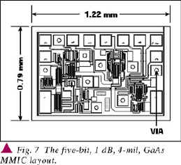
In an effort to keep the die size as small as possible, the impedance of the internal transmission lines was increased to 70W . This change allowed the width of RF lines to be reduced from 73 to 30 µm while the SWR remained less than 2 over most of the band. The resultant die size was essentially limited by the number and position of the I/O bond pads, and not the internal circuitry. Figure 7 shows the die layout; Figure 8 shows the measured results.

ASSEMBLY
Both the driver and MMIC dice are attached to the grounded paddle with epoxy. Unlike the ceramic and SOW plastic devices that contain internal circuitry, interconnections between ASIC and MMIC dies utilize direct die-to-die wirebonds. Extensive testing has shown that this method is an effective and reliable assembly technique for interconnecting die in small packages.
PRODUCT DESCRIPTION
Table 1 lists the characteristics of the AT90-XXXX attenuator family. The initial product operates with +5 and ?5 V supplies at +6 and ?1 mA (max), respectively. Logic inputs are TTL compatible. A logic 0 sets the bits to reference loss while a logic 1 selects the attenuation levels. Typical switching speed is 35 ns with rise and fall times of 5 ns.
The AT90-0001 attenuator containing the 4-mil via process die exceeded expectations and is specified to operate to 6 GHz. While DC blocks are not needed on the RF ports, 0.01 µF decoupling capacitors are required on each power supply line to ensure switching speed performance. The plastic MLP package measures 6.0 x 4.0 x 0.9 mm. Thirty-two 0.25 x 0.40 mm I/O pads are set at 10 per long side, six per short side on a 0.5 mm pitch. The 2.8 x 4.8 mm center die pad must be soldered to the PCB to ensure good RF performance.
To accommodate single power supply systems, four single-supply (+5 V at 10 mA) attenuators are presently in development. These devices will use an internal GaAs DCDC converter to produce the required negative voltage. The two previously referenced decoupling capacitors must be increased to 0.1 µF, and a third 0.01 µF coupling capacitor is required between pins 23 and 21.
Sample attenuators (AT90-XXXX) and/or test boards (AT90-XXXX-TB) are available upon request. Table 2 lists the AT90-0001 31 dB, five-bit attenuator's preliminary specifications. A test board for the device is shown in Figure 9. Figure 10 shows measured results. Full data sheets containing suggested PCB layouts are available on the company's Web site at www.macom.com.

References
1. Shmuel Ravid, Alan R. Olsen and Gary E. St. Onge, "Electronic Attenuator," US Patent 5,281,928.
M/A-COM,
Lowell, MA (800) 366-2266.